Copper wiring structure comprising a copper material buried in a hollow of an insulating film and a carbon layer between the hollow and the copper material in semiconductor device and method of fabricating the same

a technology of copper wire and insulating film, which is applied in the direction of basic electric elements, solid-state devices, thermoelectric devices, etc., can solve the problems of poor step coverage of film, difficult to form seed layers on the inner wall face of wiring grooves, and difficult to fine-tune copper processing by reactive ion etching (rie)

Inactive Publication Date: 2002-11-26
RENESAS ELECTRONICS CORP
View PDF23 Cites 12 Cited by
  • Summary
  • Abstract
  • Description
  • Claims
  • Application Information

AI Technical Summary

Problems solved by technology

In the multilayer interconnection technology, a crucial problem is to select conductive materials used for wiring and insulation materials for use as interlayer insulation films between the wiring layers.
This is because a fine processing of copper by a reactive ion etching (RIE) is difficult.
It becomes difficult, however, to form seed layers on the entire inner wall face of the wiring grooves in the conventional art as hitherto described when the wiring grooves have a fine width and large depth.
This is because, since metal films such as a TiN film or tantalum film (Ta film) to be used for seed layers are deposited by a sputtering method, step coverage of the film becomes poor thereby being difficult to completely bury copper into the wiring grooves.
As hitherto described, it becomes difficult to fabricate wiring in grooves having a large ratio between the wiring height and width, or having a high aspect ratio.

Method used


Image

  • Copper wiring structure comprising a copper material buried in a hollow of an insulating film and a carbon layer between the hollow and the copper material in semiconductor device and method of fabricating the same
  • Copper wiring structure comprising a copper material buried in a hollow of an insulating film and a carbon layer between the hollow and the copper material in semiconductor device and method of fabricating the same
  • Copper wiring structure comprising a copper material buried in a hollow of an insulating film and a carbon layer between the hollow and the copper material in semiconductor device and method of fabricating the same

Examples


first embodiment

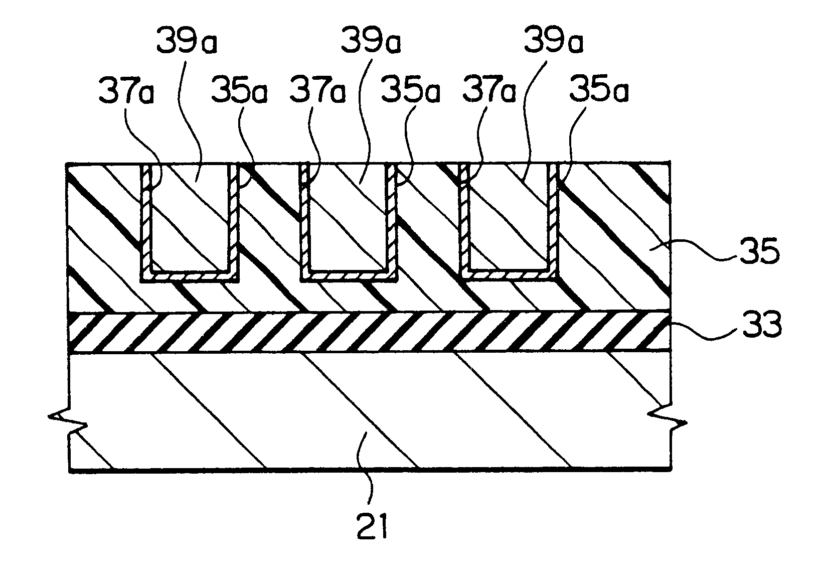
Referring to FIG. 6, the copper wiring structure according to the present invention is formed on an underlying insulation film 33 formed on the silicon substrate 21. An organic interlayer film 35 is provided on the underlying insulation film 33. The organic interlayer film 35 is provided with a plurality of wiring grooves 35a, 35a and so on. Each portion of the electroconductive carbon layers 37a is formed on the inner wall and bottom face of this wiring groove 35a. A copper wiring 39a is buried in the wiring groove 35a.

The steps of fabricating the copper wiring according to the first embodiment of the present invention will be described hereinafter.

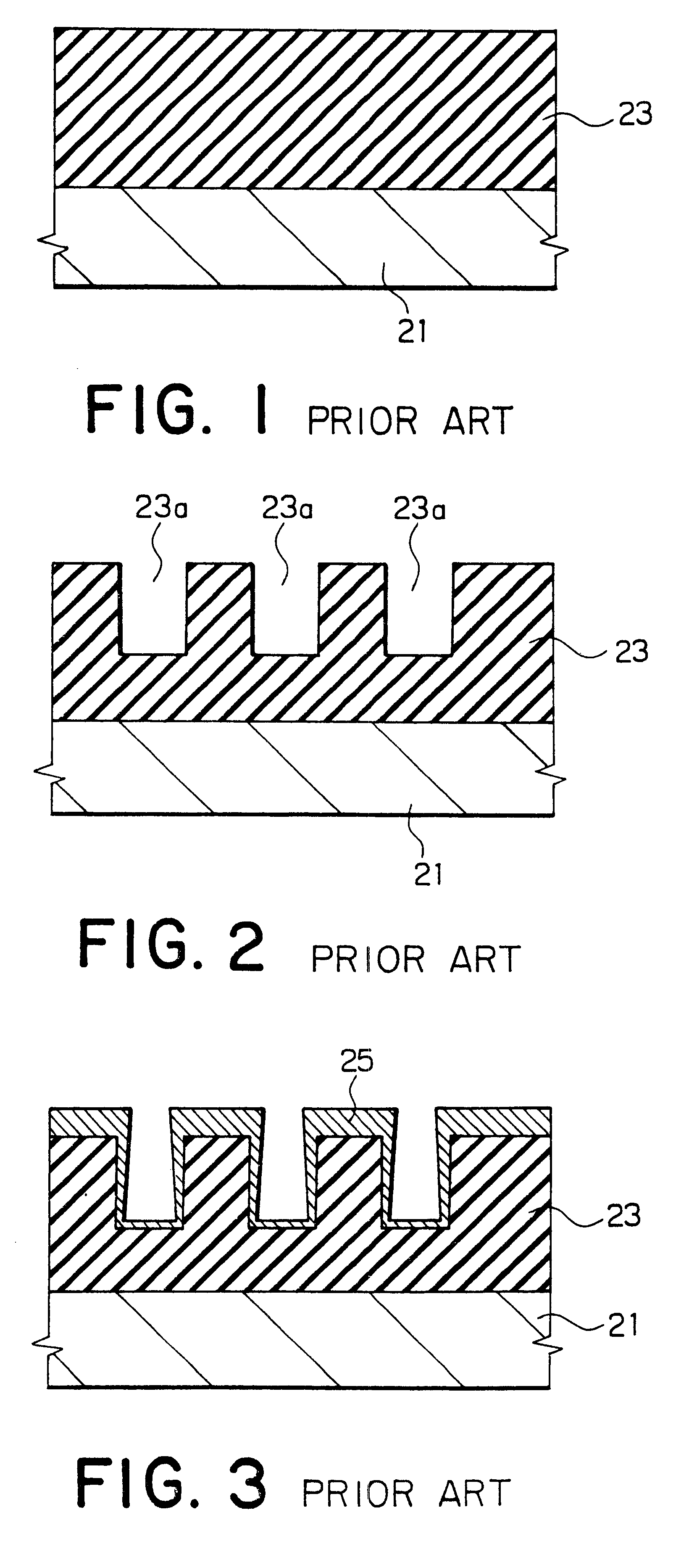
As shown in FIG. 7, the underlying insulation film 33 is flattened and is, thereafter, formed on the entire surface of the silicon substrate 21. The underlying insulation film 33 is a silicon oxide film with a thickness of about 200 nm deposited by the CVD process.

Then, an organic interlayer film 35 is formed on the underlying insulation...

second embodiment

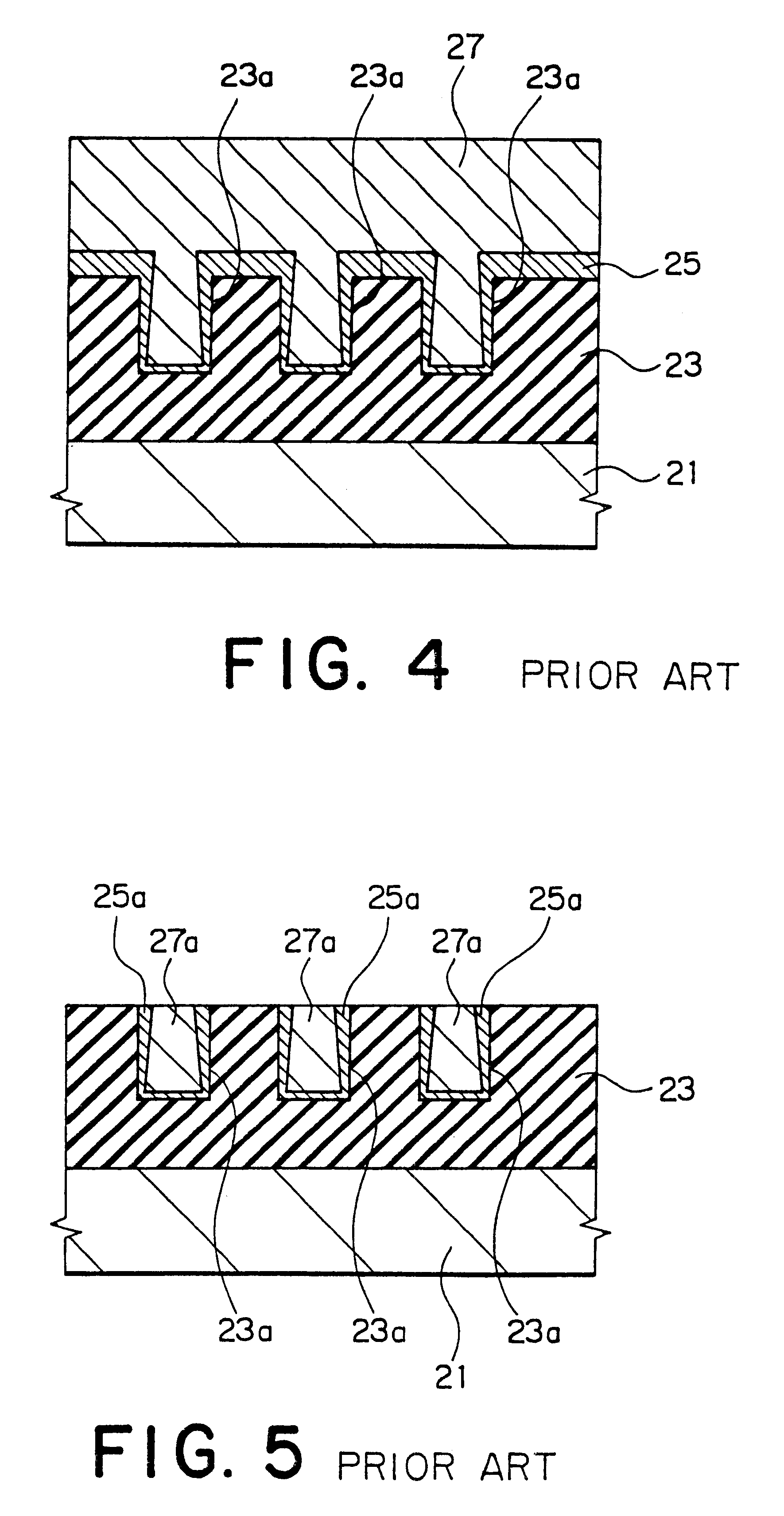
the present invention will be described hereinafter referring to FIG. 12 to FIG. 16. FIG. 12 to FIG. 16 show cross sections of the sequential production steps for selectively depositing the Cu films. The same parts as described in FIG. 1 to FIG. 11 are indicated by the same reference numerals in FIGS. 12 to 16.

Referring to FIG. 12, an underlying insulation film 33 is deposited on the silicon substrate 21, on which an organic interlayer film 35 is formed. A plurality of wiring grooves 35a are provided in the organic interlayer film 35. A conductive carbon layer is formed on the inner wall and bottom face of the wiring groove 35a. A copper wiring 47 is provided in the wiring groove 35a, the top portion of which is projected out of the organic interlayer film 35.

The method of fabricating the copper wiring structure according to the second embodiment will be described hereinafter. As shown in FIG. 13, a underlying insulation film 33 is formed on the entire surface of the silicon substra...

third embodiment

Referring to FIG. 17, a multilayer structure of the third embodiment is formed by stacking a plurality of the copper wiring layers described above. The copper wiring layers are connected to each other through via hold 35b. The via hole 35b is formed in the organic interlayer 37 and is filled with copper.

In a similar manner as described above, the via hole 35b if formed in place of the wiring groove 35a, and is changed to be conductive at a surface of the organic interlayer films 35, and is thereafter subjected to deposition of copper (Cu). The via hole 35b and the wiring groove 35b may be filled with copper individually. Alternatively, the organic interlayer 35 may be pre-shaped to form the via hole 35b and the wiring groove 35a. Thereafter, both of the via hole 35b and the wiring groove 35a may be simultaneously filled with copper as shown in FIG. 17.


PUM

PropertyMeasurementUnit
relative dielectric constantaaaaaaaaaa

Abstract

The object of the present invention is to provide a copper wiring structure in which finely processed copper wiring in a wiring structure in grooves is steadily formed with a high reliability and a method for fabricating the same, wherein an electroconductive carbon layer is formed between the copper material-a copper wiring of a wiring structure in grooves in which the copper material is buried into a wiring groove or holes formed in the organic interlayer film mainly composed of carbon-and the organic interlayer film. This electroconductive carbon layer is formed after forming wiring grooves or holes in the desired region of the organic interlayer film, by a modification of the inner wall of the wiring grooves or holes by plasma irradiation. The copper wiring of the wiring structure in grooves as described above is formed by depositing copper on the electroconductive carbon layer.

Description

1. Field of the InventionThe present invention relates to a copper wiring structure for use in a semiconductor device and a method of fabricating the same.2. Description of the Related ArtThe art for fabricating fine and highly integrated semiconductor devices has been industriously developed in resent years. Semiconductor devices currently used are fabricated in a dimensional order of about 0.13 .mu.m. Semiconductor devices, for example a memory device, such as 4 gigabit DRAM or a logic devices, use design standards based on this size and are under research and development.Three dimensional stacks of the highly integrated semiconductor elements are being investigated along with fabricating a highly integrated two dimensional device with a fine construction. For this purpose, a multilayer interconnection technology with a fine construction has became most important. In the multilayer interconnection technology, a crucial problem is to select conductive materials used for wiring and ...

Claims


Application Information

Patent Timeline
Patent Type & Authority Patents(United States)
IPC IPC(8): H01L21/02H01L23/532H01L21/768H01L21/70H01L23/52H01L21/314H01L21/3205H01L21/3213H01L23/522
CPCH01L21/3146H01L21/76802H01L21/76814H01L21/76823H01L21/76826H01L21/76843H01L21/76867H01L21/76876H01L21/76879H01L21/7688H01L23/53238H01L2924/12044H01L2924/0002H01L2924/00H01L21/0217H01L21/02205H01L21/02274H01L21/02115H01L23/53228
Inventor UENO, KAZUYOSHI
Owner RENESAS ELECTRONICS CORP
Why Eureka
Try Eureka