

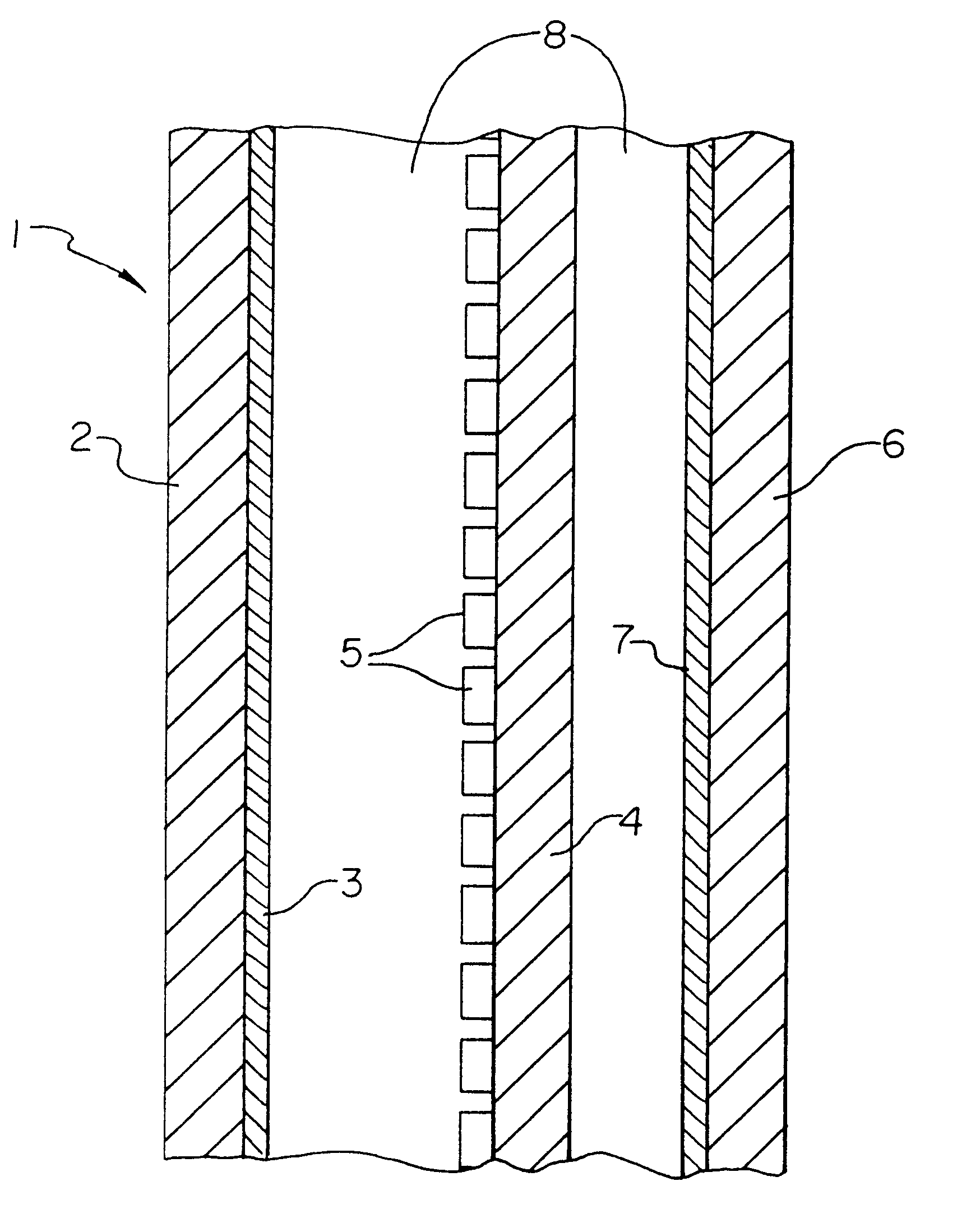
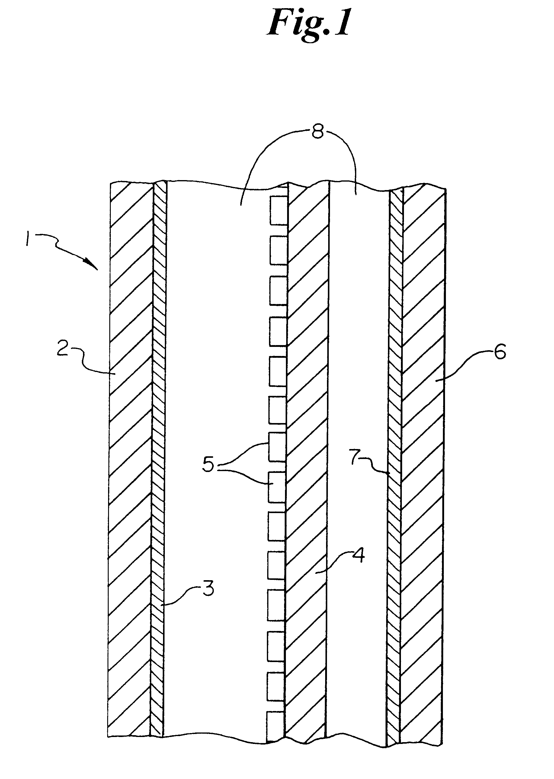
Radio wave absorbing panel
a technology of radio wave and absorber, which is applied in the direction of electrical equipment, screening rooms/chambers, and antennas. it can solve the problems of deterioration of radio wave environment in office offices, high reflectivity of radio waves, and serious social problems
- Summary
- Abstract
- Description
- Claims
- Application Information
AI Technical Summary
Benefits of technology
Problems solved by technology
Method used
Image

Examples
second preferred embodiment
An indium tin oxide (ITO) sintered target was mounted in an in-line sputtering apparatus and a gas made by adding 20 mol % oxygen to Ar was introduced to form an ITO film of thickness about 60 nm on a soda lime silica glass substrate of thickness 4 mm. The film-forming conditions were controlled so as to bring the sheet resistivity of the film to about 400.OMEGA. / .quadrature..
A laminate was made by substituting this substrate for the substrate having the CrOxNy film formed thereon of the first preferred embodiment and the radio wave reflectivity and transmittivity from 200 MHz to 1 GHz of this laminate were measured. The result was that the laminate exhibited substantially the same characteristics as the first preferred embodiment.
third preferred embodiment
Using an in-line sputtering apparatus, SnO.sub.2, Ag and SnO.sub.2 films were formed on a soda lime silica glass substrate of thickness 4 mm. The film thicknesses were respectively controlled to 40 nm, 15 nm and 40 nm, and a film of sheet resistivity 5.OMEGA. / .quadrature. was obtained.
The film face of this glass substrate was scored in a checkerboard pattern using a steel needle and thereby divided up into squares of side length about 20 cm. When the divisions were viewed with an optical microscope the film was seen to have been cut away in lines of just under 200 .mu.m in width. The electrical resistance between adjacent conducting films thus divided was generally over about 50k.OMEGA.. A laminate was made by substituting this glass substrate with films in the form of a matrix of 20 cm squares formed thereon for the glass substrate having the matrix of ZnO / Ag / ZnO films formed thereon of the first preferred embodiment, and the radio wave reflectivity and transmittivity from 200 MHz ...
fourth preferred embodiment
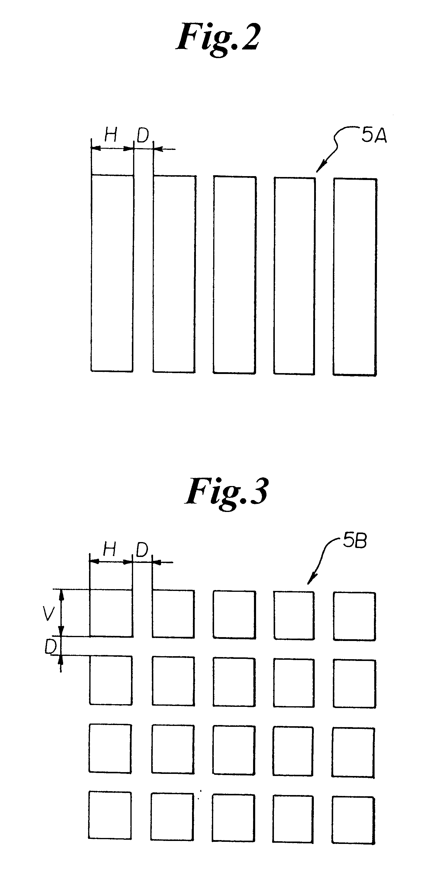
The Cr oxide nitride film CrNxOy of sheet resistivity about 400.OMEGA. / .quadrature. mentioned in the first preferred embodiment was formed on glass of thickness 10 mm and this was cut into a square of side length 80 cm and stood perpendicular to a floor surface.
Cubes of foam styrol of side length 1 cm were then affixed to the film face side of this glass as spacers at lattice points about 30 cm apart.
Colorless float glass of plate thickness 4 mm coated with a transparent conducting film consisting of an SnO.sub.2 film of sheet resistivity about 10.OMEGA. / .quadrature. doped with fluorine of film thickness about 300 nm was cut into strips of width 20 cm, length 180 cm, and these were lined up closely in the longitudinal direction on a plate of plastic and fixed to make a panel of side length 180 cm.
This panel was stood vertical and placed against the 10 mm-thick glass with the foam styrol spacers therebetween.
Also, so as to sandwich this panel and parallel therewith another panel havi...
PUM
 Abstract
Description
Claims
Application Information