Information storage element, manufacturing method thereof, and memory array

a technology of information storage and manufacturing method, applied in the direction of digital storage, instruments, semiconductor devices, etc., can solve the problems of memory not being able to operate as a non-volatile memory, unable to meet the requirements of writing time, etc., and achieve high speed and high reliability memory

Inactive Publication Date: 2006-03-09
JAPAN SCI & TECH CORP
View PDF22 Cites 14 Cited by
  • Summary
  • Abstract
  • Description
  • Claims
  • Application Information

AI Technical Summary

Benefits of technology

[0012] Also, the floating gate layer may have the structure to sandwich a polycrystal silicon thin film layer with silicon oxide layers. Also, the each thickness of the two silicon oxide layers sandwiching a polycrystal silicon thin film layer may be different each other. According to this make-up, the elastic modulus of the floating gate can be varied in the every deflective direction, so that, for example, the writing speed can be made higher. The floating gate layer instead of the above mentioned is preferably a laminated structure of a silicon oxide layer and silicon nitride layer. According to this make-up, since the electric charges are held at defect states of the interface between the silicon oxide layer and the silicon nitride layer, the injected charges of the floating gate are well stored, and are not changed by the writing voltage.
[0019] And another assumption may be possible as follows. Upon generating the thermal expansion of floating gate layer by the annealing, since the thermal expansion coefficient of silicon oxide is positive, the floating gate layer expands sufficiently as a volume relaxation by the thermal treating and the influence of the space of cavity. And since the expansion in the direction of film thickness is small enough, the floating gate layer may extend effectively in the direction of channel length. In this case, since the volume of the gate insulation film holding the floating gate layer and the substrate holding the gate insulation film are relatively or sufficiently large, the expansion of those are negligible compared to the expansion of the floating gate layer, and therefore the double stable states of the floating gate layer which are advantageous in elastic energy may be generated.
[0020] Further, a memory array according to the present invention is characterized in that, it uses the information memory device described above as a memory cell. In the memory array of such makeup, since information can be written and read by mechanical operation of the floating gate, the device is not deteriorated by leak current, and is of high speed and high reliability memory.

Problems solved by technology

However, in the above-mentioned electrical flash memories, the material existing between the floating gate and the drain, through which the electric current of writing flows, is deteriorated by the current, and the repetition of the writing causes the formation of leakage current path between the floating gate and the drain, thereby a restriction for the times capable of writing arises.
That is, since the electrons or positive holes accumulated in the floating gate flow out through the leakage current path formed by the repetition, there is a problem to be solved that the repetition of writing causes the memory not to operate as a non-volatile memory.

Method used


Image

  • Information storage element, manufacturing method thereof, and memory array
  • Information storage element, manufacturing method thereof, and memory array
  • Information storage element, manufacturing method thereof, and memory array

Examples


Embodiment Construction

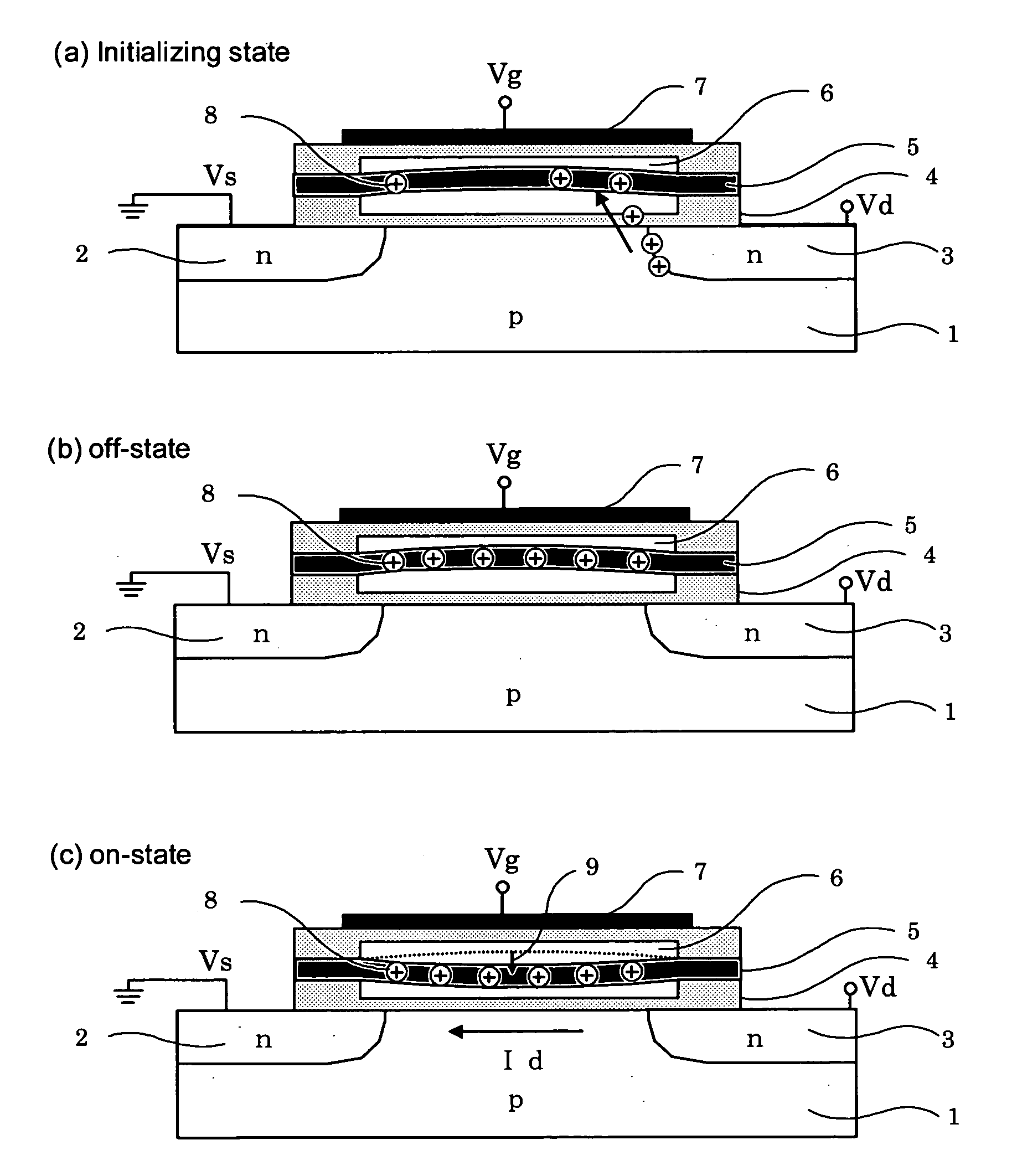
[0032] Hereinafter, the appropriate embodiments of the present invention will be described in detail with reference to the drawing figures using same marks and symbols for practically identical or corresponding parts. In the present embodiment, although accumulated carriers are assumed to be positive holes, entirely same description is possible even for the case in which accumulated carriers are electrons, by exchanging on and off states. Also in the present embodiment, although the floating gate layer is described as fixed at its both ends likely so-called supported beam, same description is possible even for the case in which the floating gate layer is fixed at its single end likely so-called cantilever.

[0033] First of all, the first embodiment of an information memory device of the present invention is explained.

[0034]FIG. 1 is a cross-sectional view of an information memory device in accordance with the first embodiment of the present invention. In order to explain the princip...


PUM


Abstract

An information memory device capable of reading and writing of information by mechanical operation of a floating gate layer, in which a gate insulation film has a cavity (6), and a floating gate layer (5) having two stable deflection states in the cavity (6), the state stabilized by deflecting toward the channel side of transistor, and the state stabilized by deflecting toward the gate (7) side, writing and reading of information can be made by changing the stable deflection state of the floating gate layer (5) by Coulomb interactive force between the electrons (or positive holes 8) accumulated in the floating gate layer (5) and external electric field, and by reading the channel current change based on the state of the floating gate layer (5).

Description

TECHNICAL FIELD [0001] The present invention relates to a flash EEPROM (electrically erasable and programmable read only memory) type non-volatile memory device belonging to one of semiconductor memory devices, a method of manufacturing the same, and a memory array of using it, especially to an information memory device characterized in the part of reading and writing of information, which are done by mechanical state change of a floating gate layer. BACKGROUND ART [0002] Heretofore, a flash memory has been known as one of non-volatile memory devices. The memory cell of the flash memory has a structure comprising a floating gate formed on a substrate via a tunnel oxide film, and a control gate formed via a gate insulation film, which are laminated with each other. In an operation of the memory cell, upon writing, electrons (or positive holes) are injected from a drain of the memory cell to the floating gate by using a voltage difference between the control gate and the drain. [0003]...

Claims


Application Information

Patent Timeline
Patent Type & Authority Applications(United States)
IPC IPC(8): H01L21/336H01L21/8247H01L27/115H01L29/788H01L29/792
CPCH01L29/7881G11C23/00H01L29/42324
Inventor YAMAGUCHI, SHINYAANDO, MASAHIKOSHIMADA, TOSHIKAZUYOKOYAMA, NATSUKIODA, SHUNRIKOSHIDA, NOBUYOSHI
Owner JAPAN SCI & TECH CORP
Why Eureka
Try Eureka