Method for cleaning semiconductor wafers

a technology for cleaning semiconductor wafers and semiconductor wafers, applied in the preparation of detergent mixture compositions, inorganic non-surface active detergent compositions, cleaning using liquids, etc., can solve the problems of hardly neutralizing the charge, affecting the cleaning effect, so as to achieve the effect of emulsification

Inactive Publication Date: 2005-06-30
PANASONIC CORP
View PDF4 Cites 16 Cited by
  • Summary
  • Abstract
  • Description
  • Claims
  • Application Information

AI Technical Summary

Benefits of technology

[0024] The acid chemical solution used in the step (c) may be prepared to have pH 2 or less. As a result, metal impurities attached to the semiconductor wafer can be effectively eluted.

Problems solved by technology

However, the conventional method for cleaning semiconductor wafers has a problem of leaving metal impurities on the semiconductor wafers.
Hence, the surfaces of the semiconductor wafers after cleaning with APM become negatively charged.
The pure water having the neutral pH can remove the residual APM but hardly neutralize the charge on the surfaces of the semiconductor wafers.

Method used


Image

  • Method for cleaning semiconductor wafers
  • Method for cleaning semiconductor wafers
  • Method for cleaning semiconductor wafers

Examples


Embodiment Construction

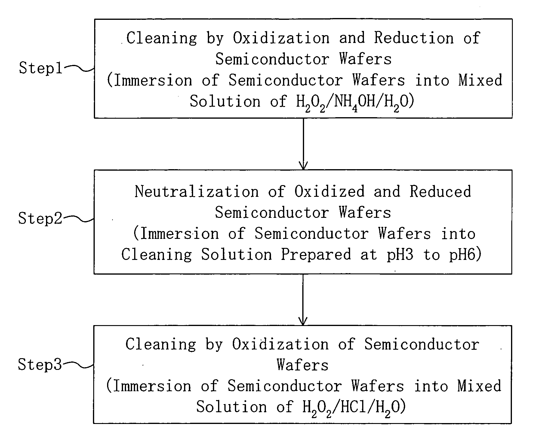
[0030]FIG. 1 is a process flow chart illustrating a method for cleaning semiconductor wafers according to an embodiment of the present invention. As shown in FIG. 1, the method for cleaning the semiconductor wafers of the embodiment includes the following first to third steps.

[0031] In the first step, the semiconductor wafers are immersed in a mixed solution of hydrogen peroxide water (H2O2), an ammonia water (NH4OH) and pure water (H2O) to clean the semiconductor wafers by their oxidation and reduction.

[0032] Next, in the second step, the semiconductor wafers after immersed in the mixed solution are immersed in a cleaning solution prepared at pH 3 to 6 both inclusive, such as an oxidized solution of any one of diluted hydrochloric acid, diluted nitric acid, diluted hydrofluoric acid and ozone water or a mixed oxidized solution of two or more kinds thereof, thereby neutralizing the surfaces of the semiconductor wafers by oxidization-reduction reaction.

[0033] Subsequently, in the ...


PUM

PropertyMeasurementUnit
pHaaaaaaaaaa
pHaaaaaaaaaa
pHaaaaaaaaaa

Abstract

A method for cleaning a semiconductor wafer according to the present invention includes the steps of: removing particles on a semiconductor wafer with an alkaline chemical solution to clean the wafer; neutralizing a surface charge of the semiconductor wafer with a weak acid cleaning solution; and removing residual metal impurities on the semiconductor wafer with an acid chemical solution to clean the wafer. The surface of the semiconductor wafer is neutralized and the HPM treatment is then performed with the semiconductor wafer having no charge. As a result, the surface of the semiconductor wafer can be made extremely clean without attaching metal impurities thereto.

Description

CROSS-REFERENCE TO RELATED APPLICATIONS [0001] The present application claims priority under 35 USC 119(a) to Japanese Patent Application No. 2003-429457 filed on Dec. 25, 2003 the entire contents of which are hereby incorporated by reference. BACKGROUND OF THE INVENTION [0002] (a) Field of the Invention [0003] The present invention relates to a process of manufacturing semiconductor wafers, especially to a method for cleaning semiconductor wafers including the steps of cleaning for removing particles with an alkaline cleaning solution and cleaning for removing metal impurities with an acid cleaning solution. [0004] (b) Description of Related Art [0005] In a process of manufacturing semiconductor devices, fine particles, metal impurities and organic impurities are attached to semiconductor wafers. Since these particles and impurities attached to the semiconductor wafers cause device malfunction, cleanliness of the semiconductor wafers is managed to a rigid standard defined therefor ...

Claims


Application Information

Patent Timeline
Patent Type & Authority Applications(United States)
IPC IPC(8): B08B3/00H01L21/304B08B3/08C11D7/00C11D7/02C11D7/08C11D11/00H01L21/302H01L21/306
CPCB08B3/08C11D7/02H01L21/02052C11D11/0047C11D7/08H01L21/304
Inventor MIYATA, TSUYOSHIMIYOSHI, YUICHINAMIOKA, YOSHIAKI
Owner PANASONIC CORP
Why Eureka
Try Eureka