Method of transferring ultra-thin substrates and application of the method to the manufacture of a multi-layer thin film device

a technology of thin film and ultra-thin substrate, which is applied in the direction of semiconductor devices, semiconductor/solid-state device details, electrical apparatus, etc., can solve the problems of affecting the thermal properties of the cube, the bulky structure of the cube, and the bulkyness of the cube, so as to achieve the effect of high density

Inactive Publication Date: 2003-01-14
INTERUNIVERSITAIR MICRO ELECTRONICS CENT (IMEC VZW)
View PDF13 Cites 180 Cited by
  • Summary
  • Abstract
  • Description
  • Claims
  • Application Information

AI Technical Summary

Benefits of technology

It is an object of the present invention to provide a method of assembly of integrated circuit chips which allows the production of the stack of such chips with high density.
It is still a further object of the present invention to provide a method of safe transfer of very thin substrates, especially semiconductor substrates.
The method may include the step of the curable adhesive being applied to the second substrate before the attaching step. The first substrate is preferably an ultra-thin semiconductor substrate formed by thinning a semiconductor substrate which is supported by the carrier and the release layer during the thinning operation. The semiconductor substrate may be provided with micro-trenches between dies which are formed on the surface to which the carrier is attached. The thinning of the semiconductor substrate should be continued until the trenches are reached. This results in an array of separated dies attached to the carrier by means of the release layer. By selective removal of these dies, the step of dicing the carrier can be avoided.
The present invention may also provide a multi-layer thin film device comprising: a plurality of layers, each layer including a planar three-dimensional interconnect portion having "X", "Y" and "Z" connection routings and adjacent thereto a planar semiconductor device portion, the semiconductor device portion being connected to the interconnect portion in each layer, the "X" and "Y" routings lying in the plane of the interconnect portion and the "Z" routing being perpendicular thereto, the "Z" routing in each interconnect portion being selectably distributed throughout the interconnect portion. A Z connection through one layer may be located at a different position than a Z connection in either the layer above or below this one layer despite the fact that the Z connections in the three adjacent layers may be connected together. The interlayer Z connections between two layers can be achieved by X or Y routings running on the surface of one of the layers. Hence, there is no need for vias going through more than one layer nor is there a need to use end or internal surfaces perpendicular to the layers for connection purposes. The Z routing through one layer is preferably achieved by means of a conductive stud which has a height substantially equal or somewhat less than the thickness of one layer, especially the thickness of an integrated circuit formed in the semiconductor portion associated with that layer. This reduces the depth of vias through insulating layers considerably which improves the accuracy of routings as deep vias with sloping walls which have a large footprint are no longer required.

Problems solved by technology

The resulting cube structure is rather bulky as each layer of the stack includes both a chip and also a carrier (semiconductor wafer) for that chip.
The above devices suffer from the problem that the cube packages are formed from relatively thick layers which not only makes them bulky but also negatively affects their thermal properties.
The handling of ultra-thin substrates, in particular semiconductor substrates such as semiconductor grade silicon, is difficult as such layers are brittle and are easily damaged.
In addition the transfer of more than one layer to form a stack is particularly difficult as the previous transferred layer does not provide a perfectly flat base such that any attempt to transfer the next ultra-thin substrate may result in damage to this layer.
This known technique makes use of aggressive chemicals and complex procedures which means that the TFT's have to be protected by special layers.
This makes the method inconvenient for commercial production.
Further, no method is described of how to stack one layer of TFT's on another to form a three-dimensional structure of active devices.
In fact, due to the use of aggressive chemicals the procedure is unsuitable for forming three-dimensional active structures.

Method used


Image

  • Method of transferring ultra-thin substrates and application of the method to the manufacture of a multi-layer thin film device
  • Method of transferring ultra-thin substrates and application of the method to the manufacture of a multi-layer thin film device
  • Method of transferring ultra-thin substrates and application of the method to the manufacture of a multi-layer thin film device

Examples


first embodiment

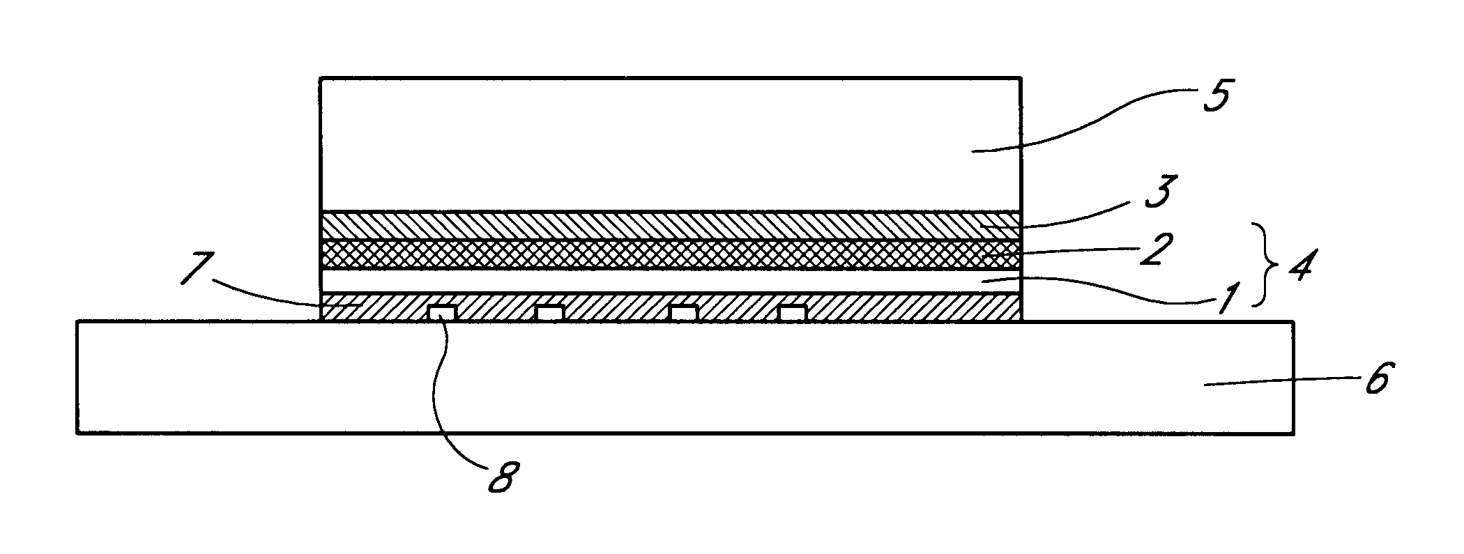
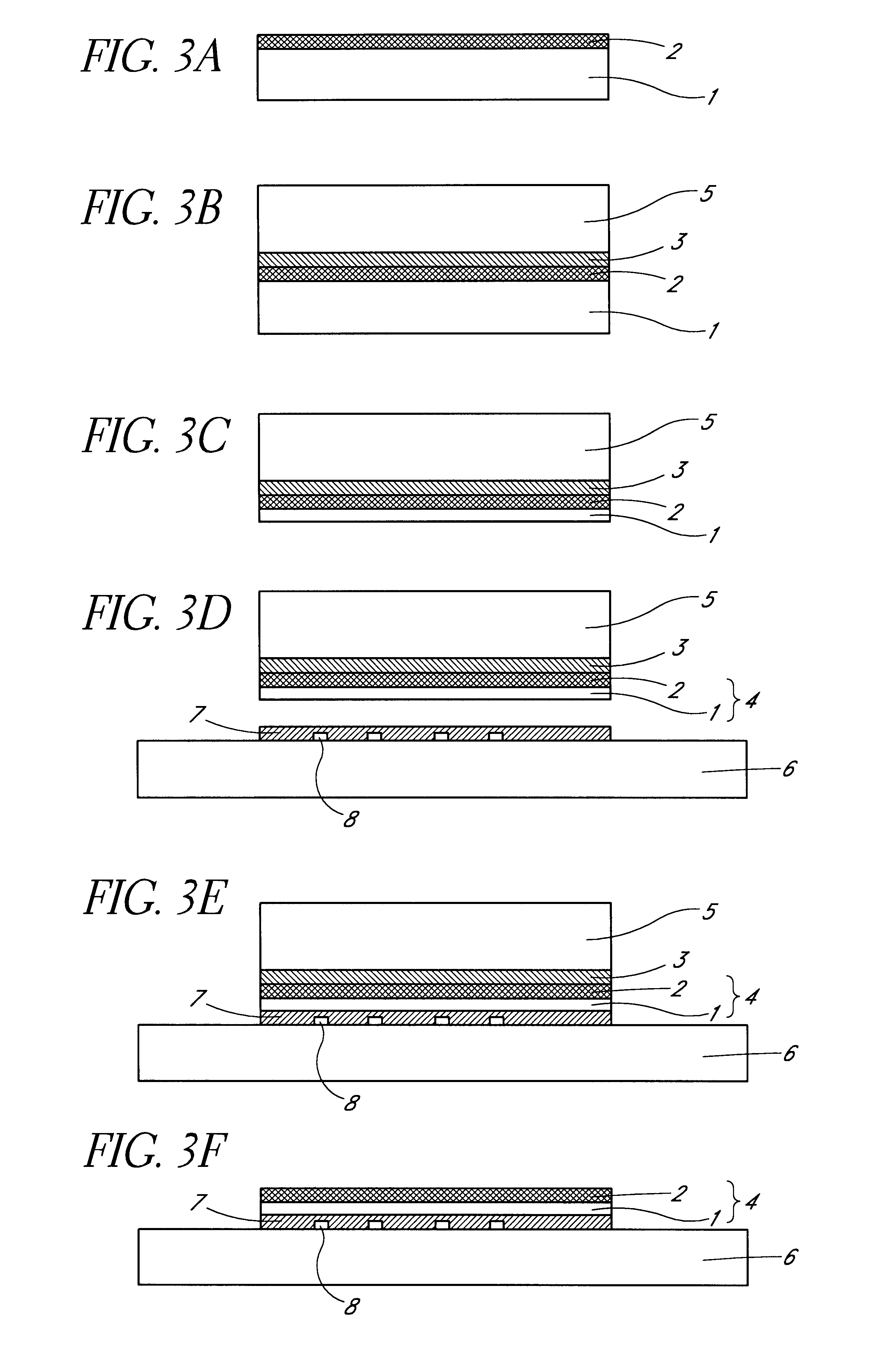
In the above description of the first embodiment the adhesive polymer layer 7 was applied to the second substrate 6 in step S3 however the present invention also includes applying the adhesive layer 7 (e.g. by spin-coating) to the surface of die 4 which has been exposed by thinning. The transfer of the die 4 to the second substrate 6 may then be carried out in accordance with steps S4 to S9 above. Note, however, that the application of the adhesive as described for step S3 is preferred as it planarises the surface of substrate 6. The planarisation of the thinned surface of the die 4 is normally achieved adequately during the thinning process of substrate 1 and therefore a further planarisation is not necessary. If necessary a polishing step may be applied after thinning substrate 1 in order to improve the planarisation of the surface of the die 4.

In accordance with a second embodiment a plurality of devices 22 are formed in a wafer 21 as shown schematically in FIG. 5A. Devices 22 ma...

third embodiment

the present invention will be described with reference to FIGS. 6A to I which is particularly useful for the production of three dimensional memory units. The starting material is a substrate 1, e.g. a semiconductor substrate, onto which is formed or deposited a layer 2 including active or passive devices (FIG. 6A), e.g. memory cells. A metallisation layer may be applied to the surface of the layer 2 of active and / or passive devices and may include one or more bonding pads 81. Substrate 1 is attached to a carrier 5 by a release layer, e.g. solvent removable photoresist, as described above (FIG. 6B). Substrate 1 is then thinned by conventional techniques, such as chemical or mechanical grinding and / or polishing, to form an ultra-thin substrate 101 which may have a thickness of about 5 to 25 micron (FIG. 6C). A second substrate 82, e.g. a semiconductor substrate, is prepared with a layer 83 of active or passive devices (FIG. 6D). An optional metallisation layer with one or more bondin...

fourth embodiment

the present invention will be described with reference to FIGS. 7A to I. The starting material is a substrate 1 with a layer 2 deposited or formed thereon or therein which may include active or passive devices. The layer 2 may also include a metallisation layer including one or more bonding pads 81. A trench 91 is then formed, e.g. by etching, ion milling or similar through device layer 2 into substrate 1 (FIG. 7A). A layer 107 of insulating material, e.g. a BCB layer is then deposited over the complete surface of the device layer 2 filling the trench 91 (FIG. 7B). The insulating layer 107 is then patterned by conventional techniques to form a via hole above the bonding pad 81. A metallisation layer is then deposited and patterned to form a metallisation strip 92 (FIG. 7C). The strip 92 extends so that it overlaps the trench 91. The top surface of insulating layer 107 is then adhered to a carrier 5 by a release layer 3 such as a solvent release layer, e.g. photoresist (FIG. 7D). Sub...


PUM


Abstract

The present invention provides a method of transfer of a first planar substrate with two major surfaces to a second substrate, comprising the steps of: forming the first planar substrate, attaching one of the major surfaces of the first planar substrate to a carrier by means of a release layer; attaching the other major surface of the first substrate to the second substrate with a curable polymer adhesive layer; partly curing the polymer adhesive layer, disconnecting the release layer from the first substrate to separate the first substrate from the camer, followed by coing the polymer adhesive layer.

Description

The present invention relates to a method of transferring ultra-thin substrates, in particular, semiconductor substrates including active devices as well as a multi-layer thin film device manufacturable using the transfer method.TECHNICAL BACKGROUNDIn order to try and increase density of packing of integrated circuits and semiconductor chips it is known to form a so called "cube" package consisting of a number of passivated device chips glued together in a stacked configuration. Conventionally these devices are connected via one of the side surfaces of the cube which is perpendicular to the layers of chips. One such known connection method is shown in FIG. 1 which is described in EP 631 310. It includes a cube of glued chips 1 with connections on one of the sides of the cube which is perpendicular to the layers of chips. The side connection connects through to the output pins 3 of a carrier 2. The cube is manufactured in the following way. Integrated circuit chips are formed on the ...

Claims


Application Information

Patent Timeline
Patent Type & Authority Patents(United States)
IPC IPC(8): H01L21/67H01L21/70H01L21/68H01L25/065H01L23/52H01L23/538H01L21/98H01L25/18H01L25/07H01L27/00
CPCH01L21/6835H01L23/5385H01L23/5389H01L24/24H01L24/82H01L25/0652H01L25/0657H01L25/50H01L2924/10253H01L2221/68354H01L2221/68359H01L2221/68363H01L2221/68368H01L2224/24226H01L2224/83192H01L2225/06513H01L2225/06517H01L2225/06524H01L2225/06541H01L2225/06551H01L2225/06593H01L2924/01004H01L2924/01013H01L2924/01029H01L2924/01033H01L2924/01039H01L2924/01075H01L2924/01077H01L2924/01078H01L2924/14H01L2924/19041H01L2924/19043H01L2924/3025H01L2924/01005H01L2924/01006H01L2924/01019H01L2924/014H01L2924/00H01L2924/351H01L2224/83005H01L2224/32225H01L2224/73267H01L2224/92244
Inventor BEYNE, ERICCOELLA-VERA, AUGUSTIN
Owner INTERUNIVERSITAIR MICRO ELECTRONICS CENT (IMEC VZW)
Why Eureka
Try Eureka