Stress control of thin films by mechanical deformation of wafer substrate

a technology of stress control and wafer substrate, which is applied in the direction of vacuum evaporation coating, coating, sputtering coating, etc., can solve the problems of film deficient or even useless for its intended function, compromising the structural integrity of the material, and forming conditions that may be detrimental to other layers of the integrated circuit devi

Inactive Publication Date: 2003-02-04
FELLOWS RES B V +1
View PDF20 Cites 50 Cited by
  • Summary
  • Abstract
  • Description
  • Claims
  • Application Information

AI Technical Summary

Benefits of technology

The methodology of the invention is also applicable in the converse to films that have little growth stress, but must be deposited at a high temperature because of the constraints of a CVD or other elevated temperature process. In such case, the thermal expansion mismatch strain can be compensated in the practice of the invention by constraining the substrate at the deposition temperature. In this way, there is little or no stress during deposition, and a stress is created during cooling, but the stress is then relieved by removing the wafer constraint.

Problems solved by technology

In the prior art fabrication of thin film materials such as metal-containing films formed by vapor phase deposition processes, including metal oxides having use in semiconductor device applications, residual stresses in the deposited thin film material can render the film deficient or even useless for its intended function.
Such residual stresses may for example interfere with desired properties of the product film, such as piezoelectric, paraelectric, superconducting, ferroelectric, and memory (in the case of memory alloy thin films) properties, and the residual stresses may compromise the structural integrity of the material, particularly in applications where the thin film is subjected to differential thermal effects or mechanical impact, vibration, etc.
However, such elevated temperature film-formation conditions may be detrimental to other layers of an integrated circuit (IC) device.

Method used


Image

  • Stress control of thin films by mechanical deformation of wafer substrate
  • Stress control of thin films by mechanical deformation of wafer substrate
  • Stress control of thin films by mechanical deformation of wafer substrate

Examples


Embodiment Construction

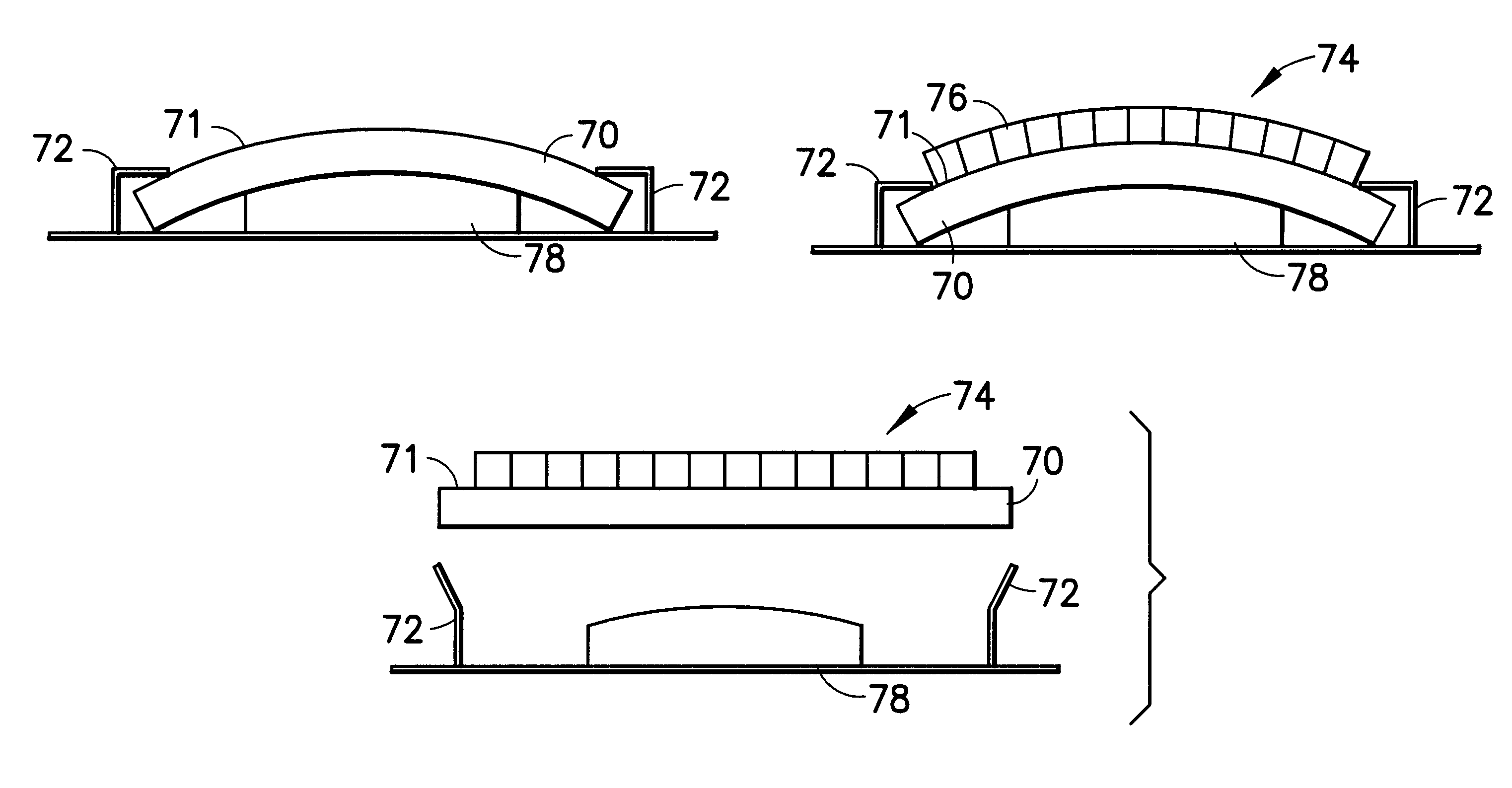
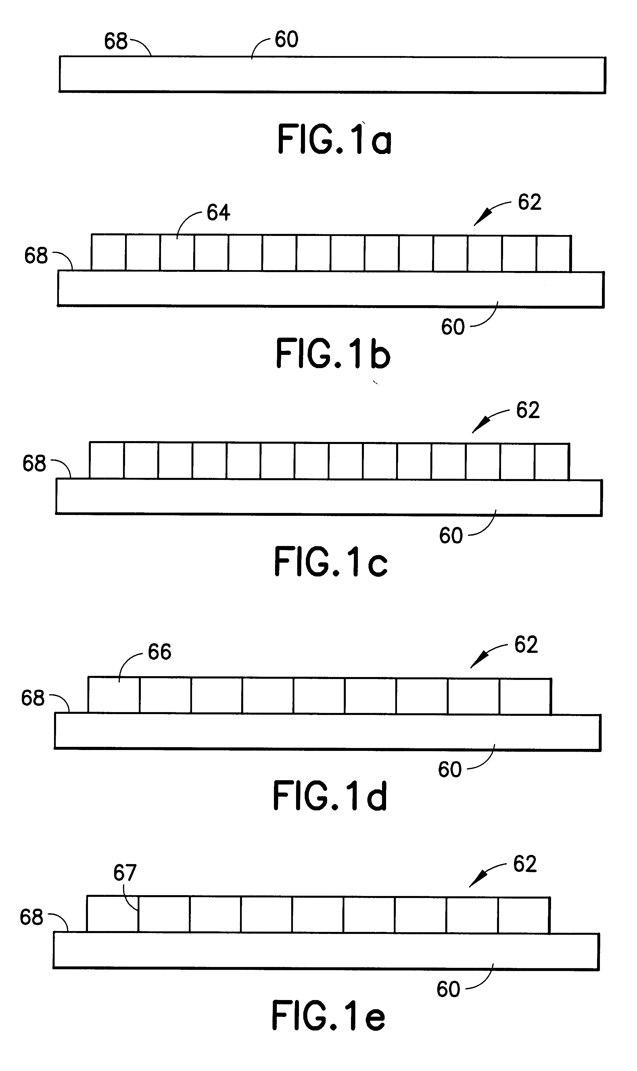
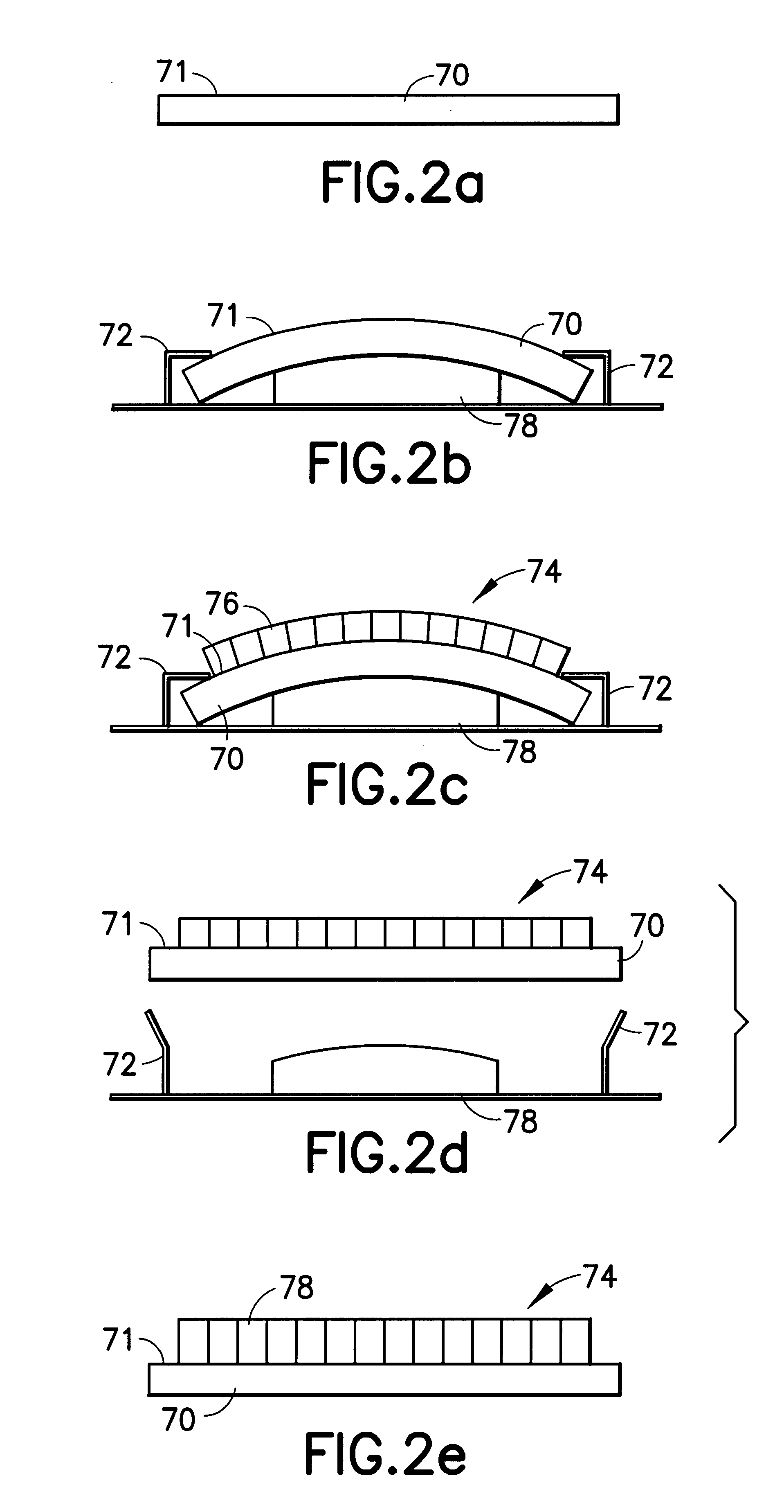
The present invention is based on the discovery that the physical, electrical, and / or magnetic properties of a thin film material, wherein such properties are stress-dependent, may be significantly improved by selectively applying force to the substrate during the film formation and / or thereafter during the cooling of the film in the case of elevated temperature film formation, for the purpose of imposing, through the substrate, an applied force condition opposing the retention or generation of stress in the product film.

In general, the stress of a thin film material (wherein "thin film" refers to films having a thickness of less than about 2000 .mu.m) may be determined quantitatively by procedures comparing films prepared with and without the use of substrate curvature, or X-ray diffraction determination of the lattice parameter at different angles with respect to the film normal. Such analyses can provide a means for comparing each resulting film stress profile against the stress ...


PUM

PropertyMeasurementUnit
Curie transition temperatureaaaaaaaaaa
thicknessaaaaaaaaaa

Abstract

A method of improving the physical and / or electrical and / or magnetic properties of a thin film material formed on a substrate, wherein the properties of the thin film material are stress-dependent, by selectively applying force to the substrate during the film formation and / or thereafter during the cooling of the film in the case of a film formed at elevated temperature, to impose through the substrate an applied force condition opposing or enhancing the retention of stress in the product film. The method of the invention has particular utility in the formation of ferroelectric thin films which are grown at temperature above the Curie temperature, and which may be placed in tension during the cooling of the film to provide ferroelectric domains with polarization in the plane of the film.

Description

1. Field of the InventionThe present invention relates to methodology for controlling the residual stresses in thin film materials formed by deposition on a substrate, and also relates to thin film structures which are characterized by reduced stress therein relative to thin films of corresponding materials produced by the prior art.2. Description of the Related ArtIn the prior art fabrication of thin film materials such as metal-containing films formed by vapor phase deposition processes, including metal oxides having use in semiconductor device applications, residual stresses in the deposited thin film material can render the film deficient or even useless for its intended function. In other cases, certain amounts of a tensile or compressive stress are beneficial.Such residual stresses may for example interfere with desired properties of the product film, such as piezoelectric, paraelectric, superconducting, ferroelectric, and memory (in the case of memory alloy thin films) proper...

Claims


Application Information

Patent Timeline
Patent Type & Authority Patents(United States)
IPC IPC(8): C23C14/54C23C14/50H01L21/302H01L21/02H01L21/316H01L41/24H01L41/257H01L41/314
CPCC23C14/50C23C14/541H01L41/314H01L21/31691H01L41/257H01L21/302H01L21/02197H10N30/045H10N30/074H10N30/508
Inventor HENDRIX, BRYAN C.ROEDER, JEFFREY F.BILODEAU, STEVEN M.
Owner FELLOWS RES B V
Why Eureka
Try Eureka