Input buffer with automatic switching point adjustment circuitry, and synchronous DRAM device including same

a digital logic and input buffer technology, applied in pulse manipulation, pulse technique, instruments, etc., can solve the problems of generating noise signals, voltage level variations of logic signals on nodes or signal lines, and unwanted noise signals occurring in and around digital logic circuits

Inactive Publication Date: 2003-02-18
MICRON TECH INC
View PDF1 Cites 41 Cited by
  • Summary
  • Abstract
  • Description
  • Claims
  • Application Information

AI Technical Summary

Problems solved by technology

Electromagnetic events occurring in and around digital logic circuits produce unwanted "noise" signals.
These unwanted noise signals may be coupled into nodes or signal lines of digital logic circuits, causing voltage level variations of logic signals on the nodes or sig

Method used


Image

  • Input buffer with automatic switching point adjustment circuitry, and synchronous DRAM device including same
  • Input buffer with automatic switching point adjustment circuitry, and synchronous DRAM device including same
  • Input buffer with automatic switching point adjustment circuitry, and synchronous DRAM device including same

Examples


Embodiment Construction

Illustrative embodiments of the invention are described below. In the interest of clarity, not all features of an actual implementation are described in this specification. It will, of course, be appreciated that in the development of any such actual embodiment, numerous implementation-specific decisions must be made to achieve the developers' specific goals, such as compliance with system-related and business-related constraints, which will vary from one implementation to another. Moreover, it will be appreciated that such a development effort might be complex and time-consuming, but would nevertheless be a routine undertaking for those of ordinary skill in the art having the benefit of this disclosure.

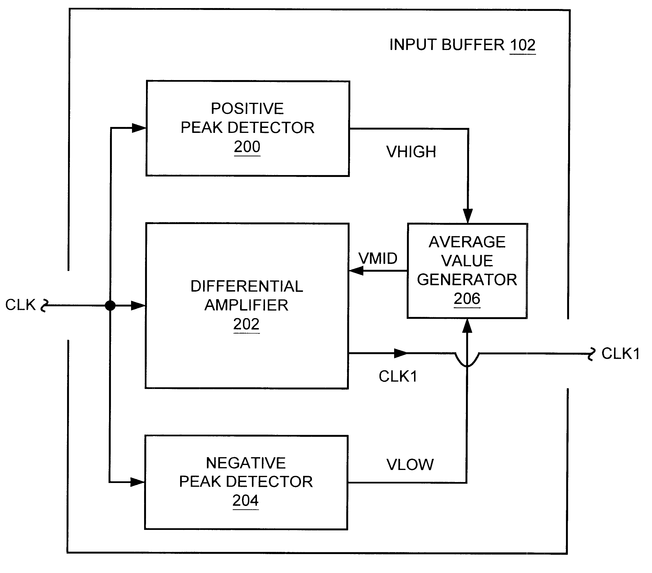
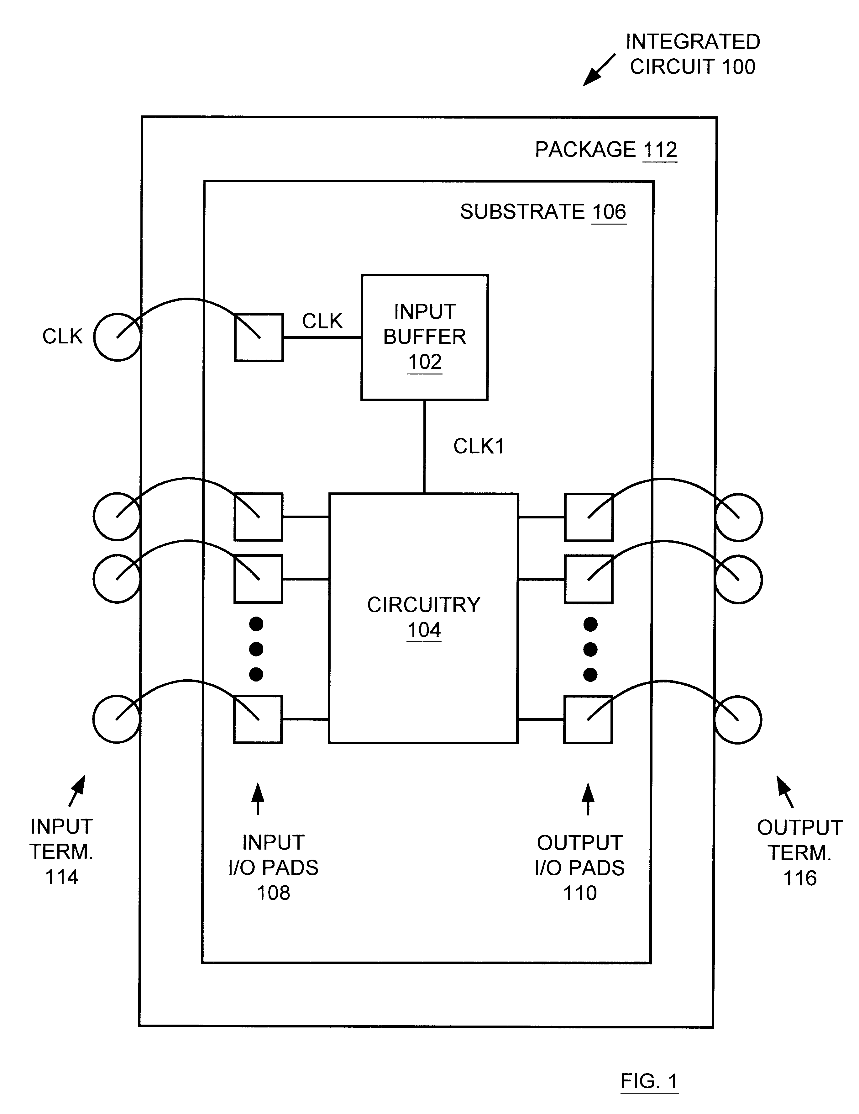
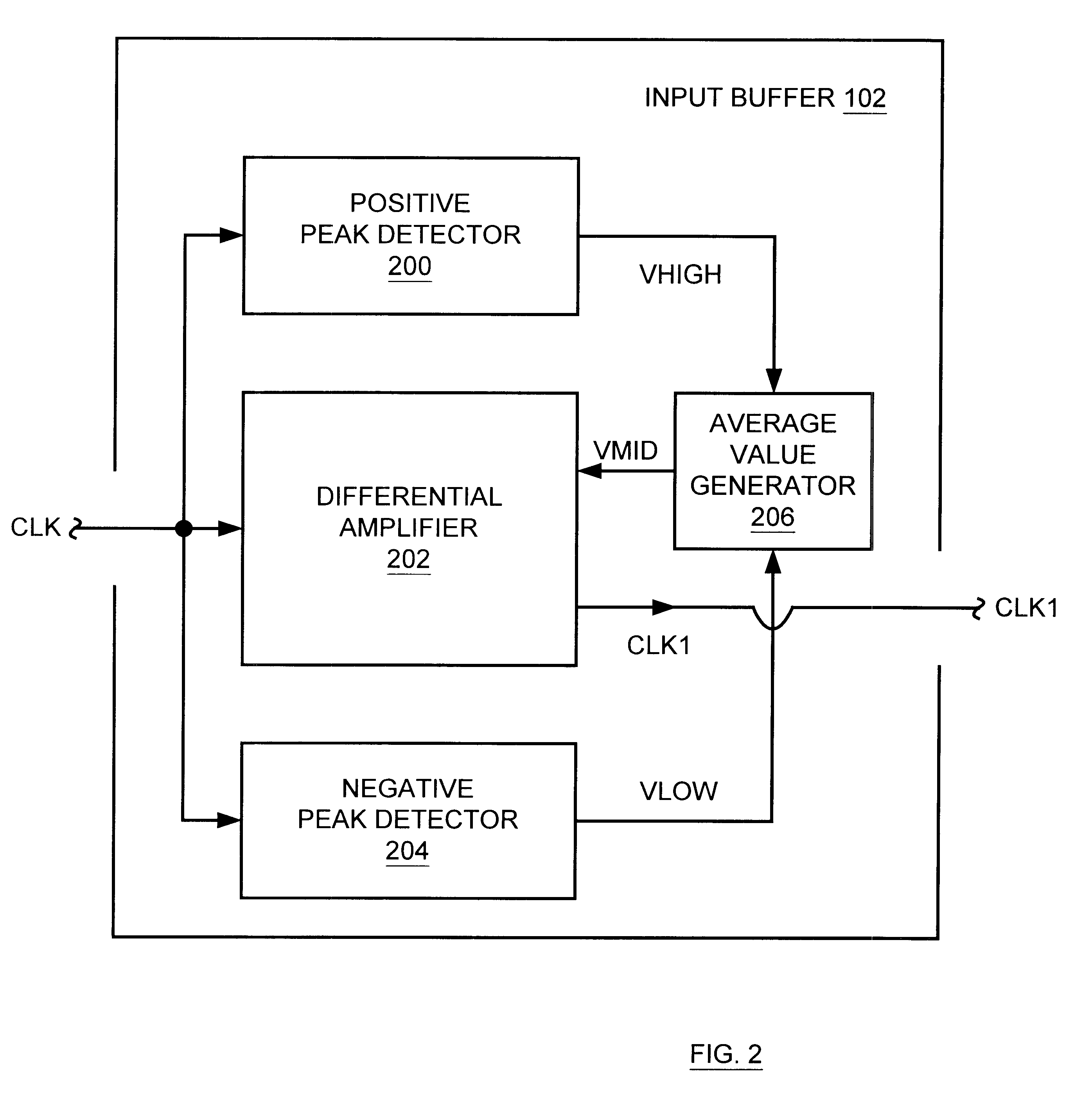
FIG. 1 is a diagram of one embodiment of an integrated circuit (IC) 100. IC 100 includes an input buffer 102, circuitry 104, and a set of electrically conductive input / output (I / O) pads, all formed upon and within a single monolithic semiconductor substrate 106. The set of I / O pads m...


PUM


Abstract

An input buffer is presented for buffering an input signal having a voltage magnitude which alternates between a first voltage level and a second voltage level, where the first and second voltage levels may vary over time. In one embodiment, the input buffer includes a first and second detector circuits, an average generator circuit, and a differential amplifier. The first detector circuit receives the input signal and produces a first signal having a magnitude indicative of the first voltage level. The second detector circuit receives the input signal and produces a second signal having a magnitude indicative of the second voltage level. The average generator circuit receives the first and second signals, and uses the magnitudes of the first and second signals to produce a third signal having a magnitude indicative of a third voltage level substantially mid way between the first voltage level and the second voltage level. The third voltage level defines a variable an automatically adjusted "switching point". The differential amplifier receives the input signal, the third signal, and a first and second power supply voltages. The differential amplifier amplifies a difference between the voltage magnitude of the input signal and the third voltage level in order to produce an output signal which alternates between the first and second power supply voltages. An integrated circuit is described including the input buffer coupled between one of a set of input/output pads and circuitry, wherein the circuitry may be synchronous dynamic random access memory (SDRAM) circuitry.

Description

1. Field of the InventionThis invention relates generally to digital logic circuits, and, more particularly, to digital logic circuits which receive signals alternating between two different voltage levels.2. Description of the Related ArtDigital logic circuits typically quantize signal voltage levels to represent two or more logic levels or states. In positive binary logic, a signal voltage level within a voltage range extending downward from a maximum operating voltage typically represents a logic "high" level (e.g., a logic `1` state), and a signal voltage level within a voltage range extending upward from a minimum operating voltage typically represents a logic "low" level (e.g., a logic `0` state).Electromagnetic events occurring in and around digital logic circuits produce unwanted "noise" signals. These unwanted noise signals may be coupled into nodes or signal lines of digital logic circuits, causing voltage level variations of logic signals on the nodes or signal lines. For...

Claims


Application Information

Patent Timeline
IPC IPC(8): G01R31/3193G01R31/28G01R31/319H03K5/08G11C7/10G11C7/22H03B1/00H03K5/156
CPCG01R31/31924G01R31/3193G11C7/1078G11C7/1084H03K5/1565G11C7/225H03K5/082H03K5/086G11C7/22
Inventor ZIVANOVIC, BRANIMIR M.
Owner MICRON TECH INC
Why Eureka
Try Eureka