Vertical metal oxide silicon field effect semiconductor diodes

a semiconductor diode and metal oxide technology, applied in the direction of diodes, semiconductor devices, electrical equipment, etc., can solve the problems of requiring careful control, affecting the performance of the diode, and only being used rarely

Inactive Publication Date: 2003-03-25
ARRAY OPTRONIX
View PDF98 Cites 34 Cited by
  • Summary
  • Abstract
  • Description
  • Claims
  • Application Information

AI Technical Summary

Benefits of technology

The features and advantages of the present invention will become apparent from the following detailed description of the present invention in which:

Problems solved by technology

However, the same are currently only rarely used, not only because of their incompatibility with silicon integrated circuit fabrication, but also even as a discrete device because of temperature sensitivity and other undesirable characteristics thereof.
In circuits which utilize the true rectifying characteristics of semiconductor diodes, the forward conduction voltage drop of the diode is usually a substantial disadvantage.
Use of a semiconductor switch to couple the secondary to the output has the advantage of a very low forward conduction voltage drop, though has the disadvantage of requiring careful control throughout the operating temperature range of the converter to maintain the efficiency of the energy transfer from primary to secondary.
The use of a semiconductor diode for this purpose has the advantage of eliminating the need for control of a secondary switch, but has the disadvantage of imposing the forward conduction voltage drop of the semiconductor diode on the secondary circuit.
First, the forward conduction voltage drop of the semiconductor diode device can substantially reduce the efficiency of the converter.
In the case of a 3 volt power supply, the imposition of a 0.7 volt series voltage drop means that the converter is in effect operating into a 3.7 volt load, thereby limiting the efficiency of the converter to 81%, even before other circuit losses are considered.
Second, the efficiency loss described above represents a power loss in the diode, resulting in the heating thereof.
This limits the power conversion capability of an integrated circuit converter, and in many applications requires the use of a discrete diode of adequate size, increasing the overall circuit size and cost.
Here two diode voltage drops are imposed on the peak DC output, making the circuit particularly inefficient using conventional diodes, and increasing the heat generation of the circuit requiring dissipation through large discrete devices, heat dissipating structures, etc. depending on the DC power to be provided.
Further, while reverse current leakage is always undesirable and normally must be made up by additional forward conduction current, thereby decreasing circuit efficiency, reverse current leakage can have other and more substantial deleterious affects on some circuits.

Method used


Image

  • Vertical metal oxide silicon field effect semiconductor diodes
  • Vertical metal oxide silicon field effect semiconductor diodes
  • Vertical metal oxide silicon field effect semiconductor diodes

Examples


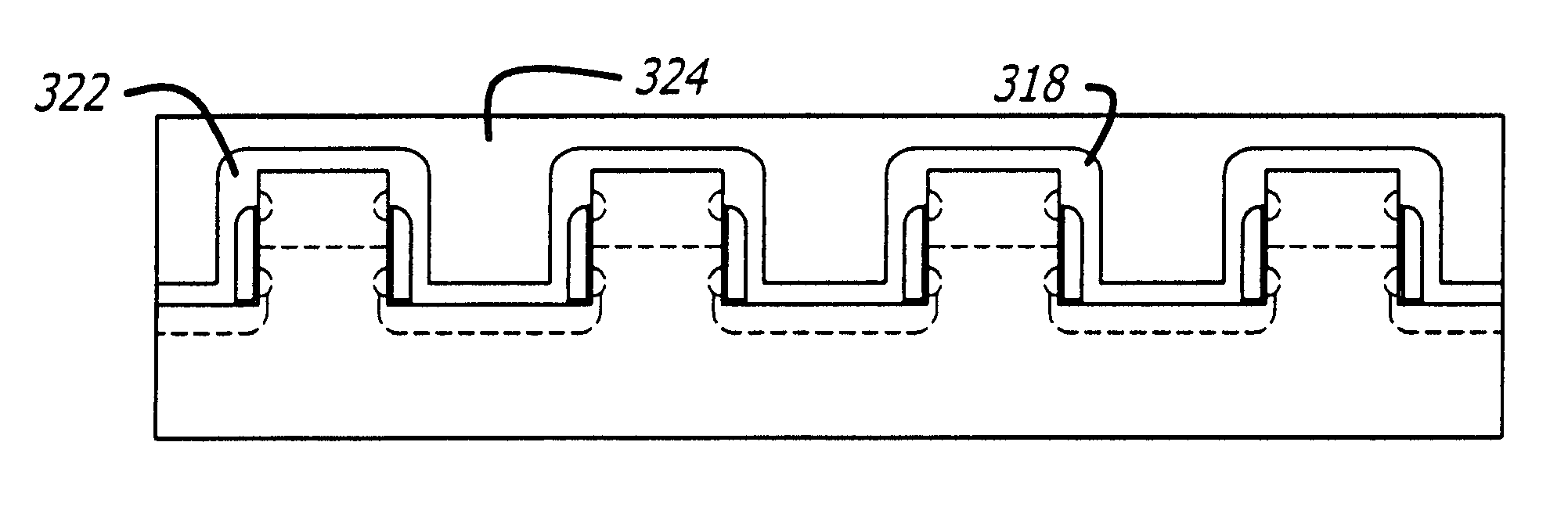
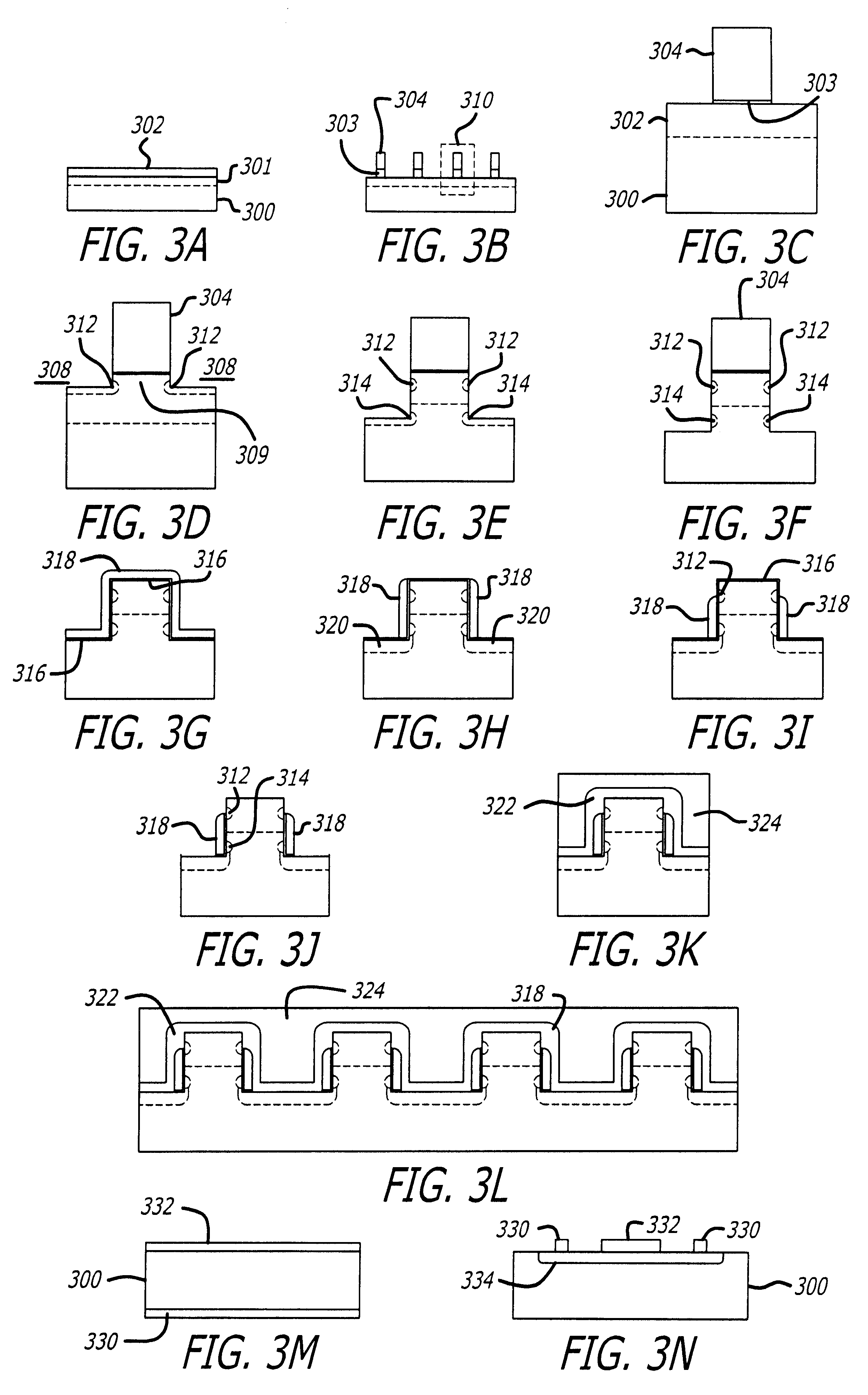
Embodiment Construction

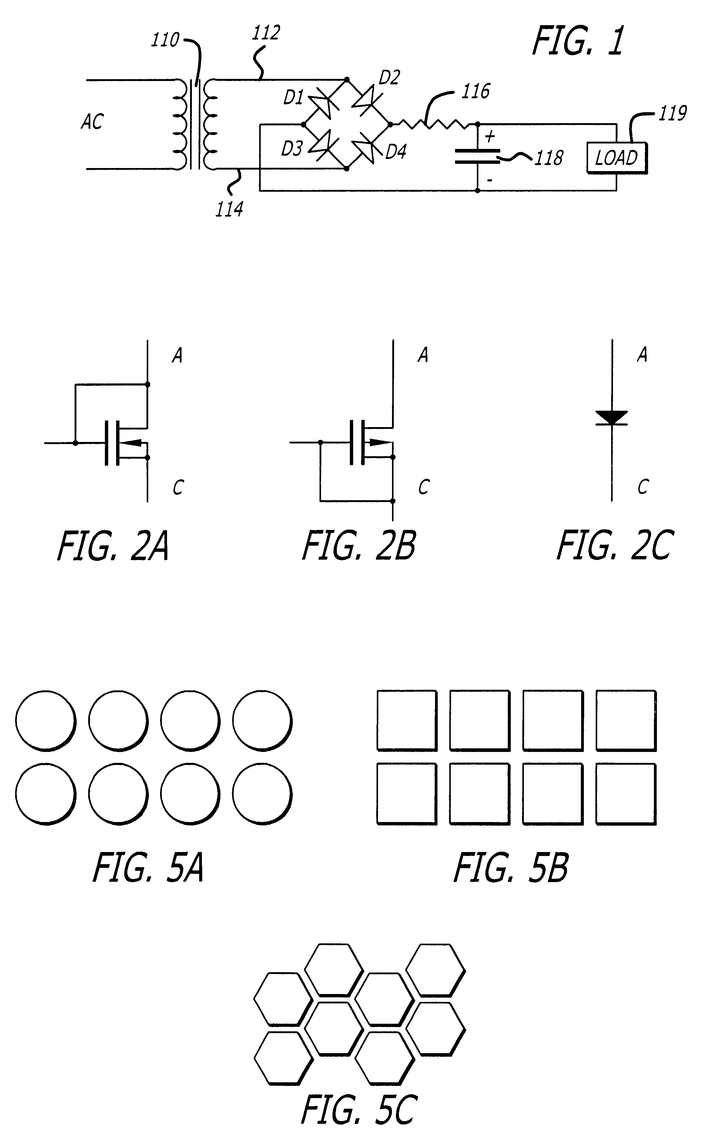
First referring to FIG. 1, a circuit diagram for a well known AC to DC converter using a full wave bridge rectifier in which the present invention may be used may be seen. In such circuits, a transformer 110 is used to provide DC isolation between the primary and secondary circuits and frequently to provide an AC voltage step-up or step-down to the full wave bridge, comprised of diodes D1, D2, D3 and D4. When the secondary lead 112 is sufficiently positive with respect to secondary lead 114, diode D2 will conduct through resister 116 to charge or further charge capacitor 118 and to provide current to load 119, which current returns to lead 114 of the transformer through diode D3. Similarly, during the other half cycle of the AC input voltage, when the voltage on secondary lead 114 is sufficiently positive with respect to secondary lead 112, diode D4 will conduct to provide current through resistor 116 to charge capacitor 118 and to provide current to load 119, with the capacitor and...


PUM


Abstract

The present invention includes methods and apparatus as described in the claims. Briefly, semiconductor diodes having a low forward conduction voltage drop, a low reverse leakage current, a high voltage capability and avalanche energy capability, suitable for use in integrated circuits as well as for discrete devices are disclosed. The semiconductor diodes are diode configured vertical cylindrical metal oxide semiconductor field effect devices having one diode terminal as the common connection between the gates and drains of the vertical cylindrical metal oxide semiconductor field effect devices, and one diode terminal as the common connection with the sources of the vertical cylindrical metal oxide semiconductor field effect devices. The method of manufacturing the vertical cylindrical metal oxide semiconductor field effect devices is disclosed. Various device terminations can be employed to complete the diode devices. Various embodiments are disclosed.

Description

1. Field of the InventionThe present invention generally relates to semiconductor devices and fabrication of the same. The present invention more particularly relates to semiconductor diodes and their methods of fabrication.2. Background InformationSemiconductor devices of various kinds are well known in the prior art. Because the present invention relates to semiconductor diodes and how they are fabricated, the focus of this section will be semiconductor diodes.Semiconductor diodes are widely used in electronic circuits for various purposes. The primary purpose of such semiconductor diodes is to provide conduction of current in a forward direction in response to a forward voltage bias, and to block conduction of current in the reverse direction in response to a reverse voltage bias. This rectifying function is widely used in such circuits as power supplies of various kinds as well as in many other electronic circuits.In typical semiconductor diodes, conduction in the forward direct...

Claims


Application Information

Patent Timeline
Patent Type & Authority Patents(United States)
IPC IPC(8): H01L21/02H01L29/66H01L21/329H01L27/08H01L29/861H01L29/78H01L21/336H01L29/866
CPCH01L27/0814H01L29/861H01L29/66075H01L29/0619H01L29/0623H01L29/66734H01L29/7813H01L29/42312H01L29/7827
Inventor METZLER, RICHARD A.
Owner ARRAY OPTRONIX
Why Eureka
Try Eureka