Method for improving inversion layer mobility in a silicon carbide metal-oxide semiconductor field-effect transistor

a technology of metal-oxide semiconductor and inversion layer mobility, which is applied in the direction of semiconductor devices, electrical appliances, basic electric elements, etc., can solve the problems of inability to meet the requirements the state of affairs is not acceptable for a variety of current or future applications, and the performance of power devices is not high

Inactive Publication Date: 2003-05-06
VLSI TECH LLC
View PDF3 Cites 24 Cited by
  • Summary
  • Abstract
  • Description
  • Claims
  • Application Information

AI Technical Summary

Benefits of technology

According to a first aspect of the present invention, a method for improving inversion layer mobility in a silicon carbide metal-oxide semiconductor field-effect transistor (MOSFET) is provided. The method comprises the steps of: (1) providing a silicon carbide substrate; and (2) forming an oxide layer on a surface of the silicon carbide substrate in a presence of metallic impurities.
According to a second aspect of the present invention, a method for improving inversion layer mobility in a silicon carbide metal-oxide semiconductor field-effect transistor (MOSFET) is provided. The method comprises the steps of: (1) positioning a silicon carbide substrate and metallic impurities in a chamber; and (2) forming an oxide layer on a surface of the silicon carbide substrate by introducing nitrogen gas bubbled through deionized water into the chamber.
According to a third aspect of the present invention, a method for improving inversion layer mobility in a silicon carbide metal-oxide semiconductor field-effect transistor (MOSFET) is provided. The method comprises the steps of: (1) positioning a silicon carbide substrate and metallic impurities in a chamber; and (2) forming an oxide layer on a surface of the silicon carbide substrate by introducing a gaseous mixture of hydrogen and oxygen into the chamber.
According to a fourth aspect of the present invention, a method for improving inversion layer mobility in a silicon carbide metal-oxide semiconductor field-effect transistor (MOSFET) is provided. The method comprises the steps of: (1) providing a silicon carbide substrate and metallic impurities in a chamber heated to a temperature of approximately 1100.degree. C.; (2) depositing approximately 100-800 nm of a low-temperature oxide on a surface of the silicon carbide substrate; (3) introducing a gaseous mixture of hydrogen and oxygen into the chamber after the depositing step; and (4) annealing the silicon carbide substrate in argon at a temperature of approximately 950.degree. C.
Therefore, the present invention provides a method for improving inversion layer mobility in a MOSFET. Specifically, the present invention forms an oxide layer on a SiC substrate in the presence of metallic impurities to improve the oxide-substrate interface.

Problems solved by technology

This means that further refinements in device design and processing are not likely to yield substantial improvements in performance.
However, this state of affairs is not acceptable for a variety of current or future applications where silicon power-devices function with heavy operating losses.
However, SiC MOSFETs currently fabricated by researchers have shown very poor inversion layer mobility (.about.1 cm.sup.2 / Vs), which is one hundred times lower than the expected mobility value.
This results in large power dissipation and loss of efficiency, which makes SiC MOSFETs less attractive in comparison to their Si counterparts.
The lower inversion layer mobility is primarily due to the poor interface between the gate oxide and the silicon carbide substrate through which the current conduction occurs.

Method used


Image

  • Method for improving inversion layer mobility in a silicon carbide metal-oxide semiconductor field-effect transistor
  • Method for improving inversion layer mobility in a silicon carbide metal-oxide semiconductor field-effect transistor
  • Method for improving inversion layer mobility in a silicon carbide metal-oxide semiconductor field-effect transistor

Examples


Embodiment Construction

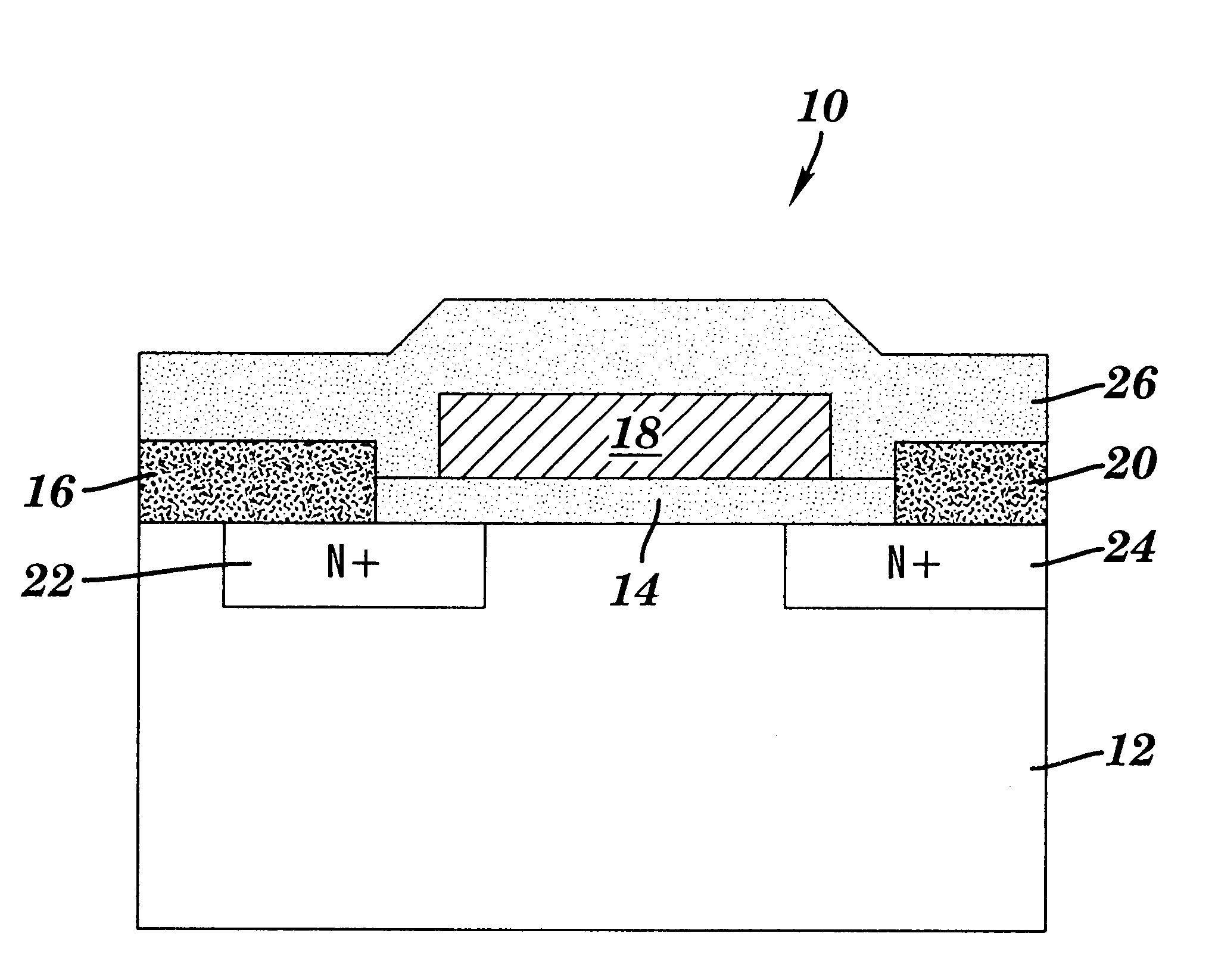
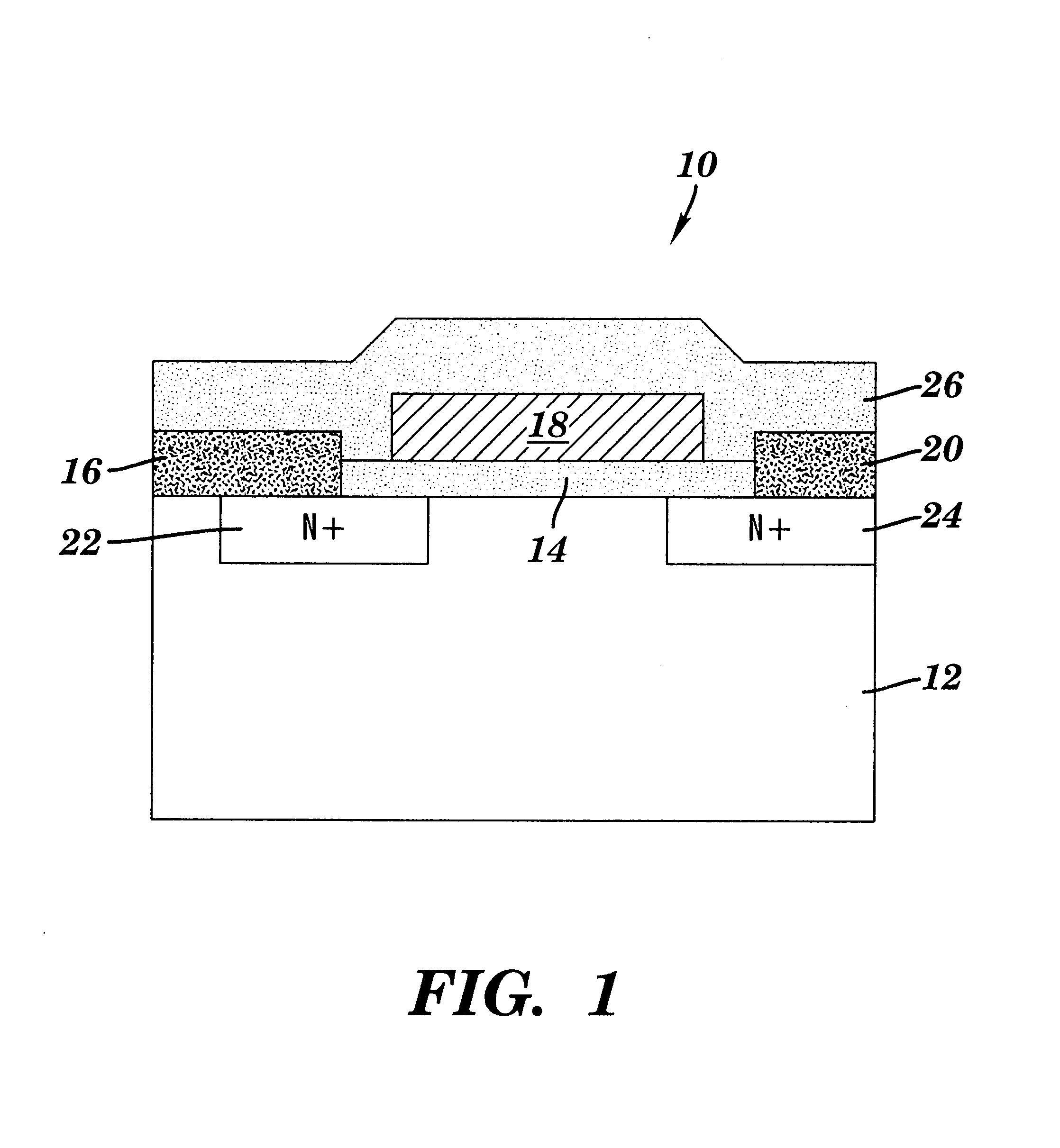
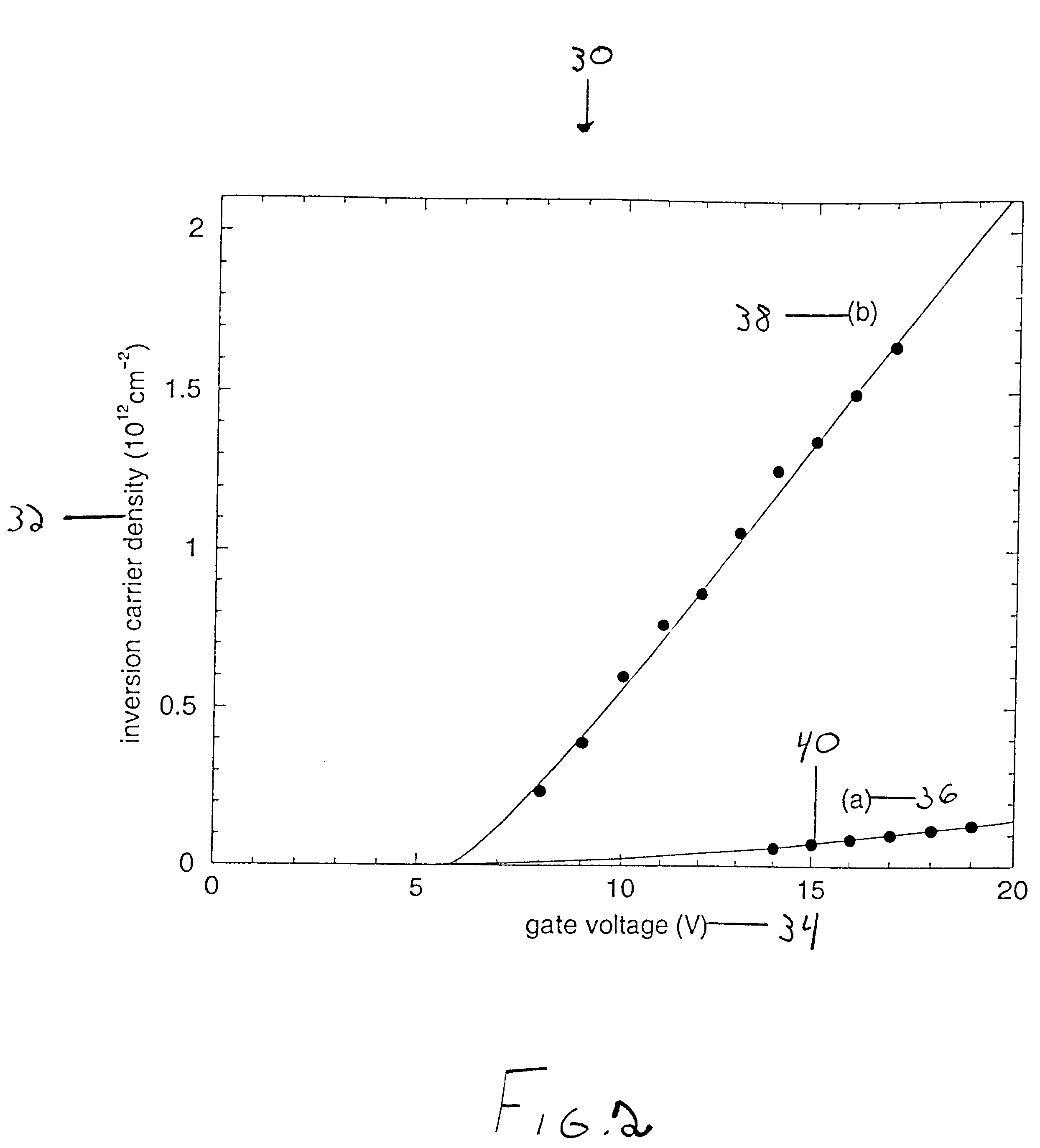
The effects of the metallic impurities of the present invention were studied on 4H-SiC lateral enhancement typed NMOS devices in which gate oxides (i.e., oxide layer 14) were prepared in two different ways. The first type of gate oxide was grown on a bare silicon carbide (substrate 12) surface in a single wet oxidation-anneal process using the following procedure:

A silicon carbide substrate was placed in a furnace, which was ramped from approximately 800.degree. C. to approximately 1100.degree. C. in an inert gas atmosphere. At approximately 1100.degree. C., the oxidation process was started by introducing a gaseous mixture of hydrogen and oxygen. In another experiment, the wet oxidation was performed by introducing nitrogen bubbled through deionized water kept at approximately 95.degree. C. Metallic impurities were introduced by placing a piece of sintered alumina containing iron impurities into the chamber. The sintered alumina contained a concentration of iron sufficient to intro...


PUM

PropertyMeasurementUnit
temperatureaaaaaaaaaa

Abstract

A method for improving inversion layer mobility in a silicon carbide metal-oxide semiconductor field-effect transistor (MOSFET) is provided. Specifically, the present invention provides a method for applying an oxide layer to a silicon carbide substrate so that the oxide-substrate interface of the resulting SiC MOSFET is improved. The method includes forming the oxide layer in the presence of metallic impurities.

Description

1. Technical FieldThe present invention generally relates to a method for improving inversion layer mobility in a silicon carbide (SiC) metal-oxide semiconductor field-effect transistor (MOSFET). In particular, the present invention relates to forming a gate oxide on SiC substrate in the presence of metallic impurities to yield a MOSFET with improved inversion layer mobility.2. Background ArtSilicon (Si) is, and has been, the most popular and widely used semiconductor material for the past thirty years. During this time, Si device technology has reached an advanced level because of constant refinements and improvements. The result of this constant improvement has brought silicon power devices to such levels of efficiency that they are now approaching the theoretical maximum power limit predicted for this material. This means that further refinements in device design and processing are not likely to yield substantial improvements in performance. However, this state of affairs is not ...

Claims


Application Information

Patent Timeline
Patent Type & Authority Patents(United States)
IPC IPC(8): H01L21/04H01L21/02H01L29/78
CPCH01L21/049H01L21/18
Inventor ALOK, DEVARNOLD, EMILEGLOFF, RICHARDMUKHERJEE, SATYENDRANATH
Owner VLSI TECH LLC
Why Eureka
Try Eureka