Package structure of full color LED form by overlap cascaded die bonding

a cascaded die bonding and pack structure technology, applied in the direction of semiconductor/solid-state device manufacturing, electrical equipment, semiconductor devices, etc., can solve the problems of short life of leds, difficult to obtain control accuracy, and not meeting the needs of the market, so as to increase heat dispersion efficiency and reduce power consumption

Inactive Publication Date: 2003-05-13
HEN CHANG HSIU
View PDF7 Cites 280 Cited by
  • Summary
  • Abstract
  • Description
  • Claims
  • Application Information

AI Technical Summary

Benefits of technology

Another object of the present invention is to provide an overlap cascaded packaging structure of a full color semiconductor LED with reflected metal layer to enhance the intensity of light.
Another object of the present invention is to provide a light source with metal oxide transparent conductive layer to die bond multi-chip to form overlap cascaded packaging structure. The structure has good resolution and is satisfied for both near field or far field observation.
The other object of the present invention is to provide an overlap cascaded packaging structure of a full color semiconductor LED to obtain light source of different colors by controlling the magnitude of the current to control the intensity of the lights, this can achieve less power consumption and increase heat dispersion efficiency.

Problems solved by technology

The control accuracy is difficult to obtain, and the design of the power control IC is complicated, more ever, for constant current much heat generated and heat dispersion is not easy, it causes short lifetime of the LED.
In near field observation, three colors is still observed, full color can be observed only for far field observation, so it does not satisfy the need of the market.

Method used


Image

  • Package structure of full color LED form by overlap cascaded die bonding
  • Package structure of full color LED form by overlap cascaded die bonding
  • Package structure of full color LED form by overlap cascaded die bonding

Examples


first embodiment

Hereunder, an overlap cascaded three primary color dice packaging structure of a full color LED according to the present invention is described with reference to the attached drawings.

The LED dice used in this invention can be made with different type of material. The dice can be made by a conventional method accordance to the specification of this invention such as chip size, bias voltage, intensity, color and metal contact, etc. The dice should be tested and classified before packaging.

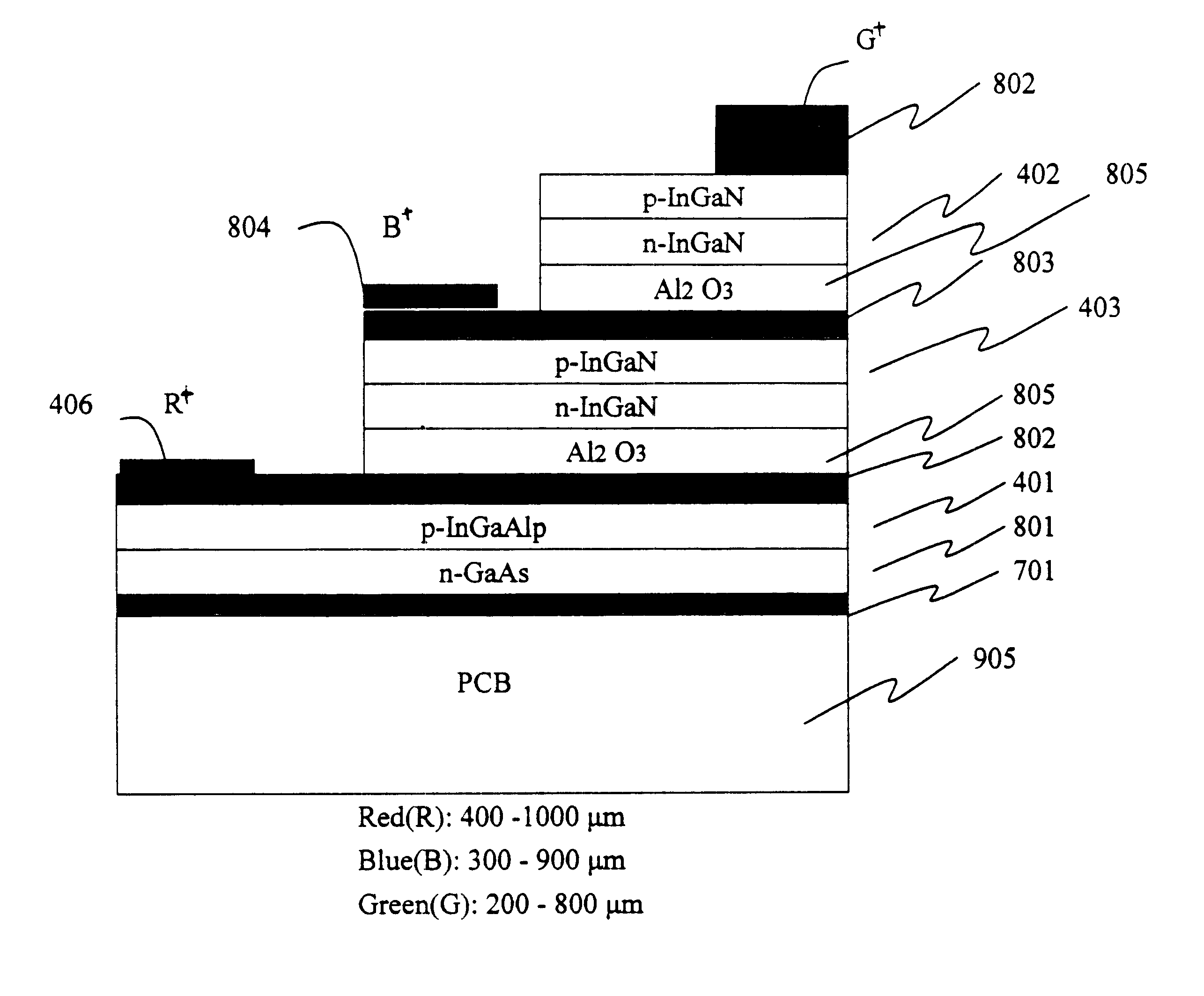
In the following embodiments, a pc-board with reflective metal pattern on the pc-board for die bonding, after the first chip is bond on the pc-board, a second chip is overlap and cascaded bond on the first chip. Bonding can be thermal, ultrasonic or transparent epoxy adhesion. A third chip is also over lap and cascaded bond on the second chip. Wire bond is then connected the positive electrode to the source and the negative electrode to the ground.

FIG. 7 shows the top view of an overlap cascaded thr...

second embodiment

an full color LED packaging structure according to the present invention is made by overlap cascaded bonding of a yellow and a blue light LEDs in parallel with another overlap cascaded red and green light LEDs. This structure is suitable for far field observation and is described in FIG. 12 and FIG. 13. FIG. 12 is the plane view. FIG. 13 is the cross section along A--A line in FIG. 12. In order to simplify die bond and save energy, we do not use three primary color LEDs, instead we use only two LEDs in overlap cascaded, then package in parallel side-by-side with another two LEDs in overlap cascaded. This structure satisfy far field observation. Refer to FIG. 13, a reflective metal layer 801(aluminum, copper or gold) with thickness of 1000 .ANG. to 20000 .ANG., the better of 2000 .ANG. to 5000 .ANG. is sputtered, evaporated or plated on a pc-board 405. Then prepare a first red LED chip 401, made by epitaxy a p-type InGaAlP on an n-type GaAs substrate with a traditional technology. On...

third embodiment

The third embodiment does not limit to overlap cascaded package of the yellow and blue LED chips or the red and green LED chips, any two complementary color with which obtain a white light after mixed can be used. The materials used to fabricate the red, green, blue and yellow LEDs are not limited to the above materials, the structure of the diode is not limited to pn-junction structure, those advance technology such as quantum well structure can be used.


PUM


Abstract

The present invention discloses a light source of full color LED (light emitted diode) by using die bond and packaging technology. A first mono-color LED chip with reflective metal on the bottom and transparent metal-oxide on the top of the chip is bonded on the PC board by thermal or ultrasonic die bond. A second mono-color LED chip with reflective metal on both sides is bonded in cascade on the first LED chip by thermal or ultrasonic die bond. The first LED chip emits light through the transparent metal-oxide to mix with the second LED light such that a different color light will obtain. The reflective metal reflects all the light to enforce the light intensity. In near field application, a red, a blue and a green LED are die bond in cascade to get a white light or full color light. In far field application, a yellow and a blue LED are die bond in cascade on the PC board, in its side is another cascaded die bond of a red and a green LED to get a white light or full color light.

Description

1. Field of the InventionThe present invention related to a packaging structure of LED and more particularly, to a package structure of overlap bonding the LEDs in cascaded by chip direct bounding with transparent conductive layer and reflected metal layer, and capable of generating a full color light or white light by mixing lights emitted from the overlap LEDs.2. Description of Relative Prior ArtAs a good light source and device made by semiconductor material, LEDs possesses advantages of small size, long life-time, low driving voltage, rapid response, and good oscillation-proof, etc.By changing the semiconductor materials and device structures, LEDs with different visible and invisible colors can be designed, wherein AlGaAs, InGaAlP and InGaN are suitable for producing LEDs with high luminance over 1000 mcd.When producing red or infrared LEDs with high luminance by AlGaAs, an LPE process and DE structure devices are used for industrial mass production.InGaAlP can be used to produ...

Claims


Application Information

Patent Timeline
Patent Type & Authority Patents(United States)
IPC IPC(8): H01L25/075
CPCH01L25/0753H01L25/0756H01L2924/0002H01L2924/00
Inventor HEN, CHANG HSIU
Owner HEN CHANG HSIU
Why Eureka
Try Eureka