Method for manufacturing a built-up circuit board

a built-up circuit board and manufacturing method technology, applied in printed circuit assembling, resistive material coating, metallic material coating process, etc., can solve the problems of reducing the adhesion strength of the metal plated layer, which is formed later, adversely affecting the environment, etc., to achieve more reliable built-up circuit boards, stable and uniform effects

Inactive Publication Date: 2003-09-02
GLOBALFOUNDRIES US INC
View PDF6 Cites 10 Cited by
  • Summary
  • Abstract
  • Description
  • Claims
  • Application Information

AI Technical Summary

Benefits of technology

It is another, more specific object of the present invention to provide an innovative resin softening process to replace the conventional swelling process that more stably and uniformly softens the surface of a resin insulating layer.
It is yet another object of the present invention to provide a more reliable built-up circuit board by increasing the adhesive strength of the bond between a metal plated layer and a resin insulating layer, by more stably and more uniformly softening the surface of the insulating layer.
It is still an additional object of the present invention to prevent the swelling process liquid from adversely affecting the environment, by reducing the amount of the fluid that is required.

Problems solved by technology

(a) Since stable performance of the swelling process is not easily predictable, the surface of the resin layer often is not uniformly (evenly) softened. As a result, during the oxidization process the surface of the resin layer is not uniformly oxidized and etched, and the strength of the adhesion acquired by the metal plated layer, which is formed later, is reduced in some areas. To reduce this unstable swelling, frequently the effects (the state of the softened surface) of the swelling process must be examined, and / or the composition of the processing liquid adjusted.
(b) Since the processing liquid that is used contains an aqueous organic solvent and a strong alkali, such as calcined soda, it is normally applied at a temperature of 40 to 100C., to prevent the generation of a solvent steam that can adversely affect the environment.

Method used


Image

  • Method for manufacturing a built-up circuit board
  • Method for manufacturing a built-up circuit board
  • Method for manufacturing a built-up circuit board

Examples


Embodiment Construction

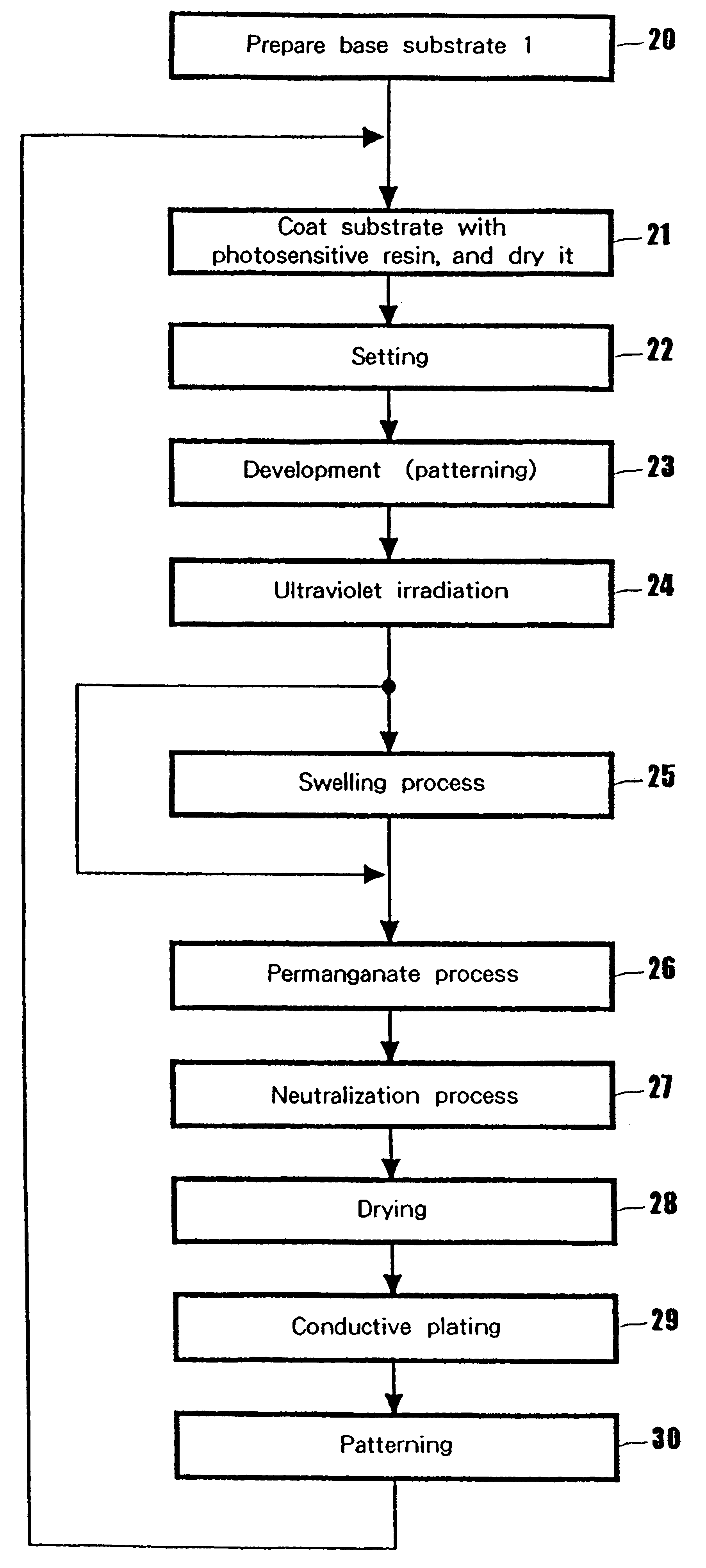
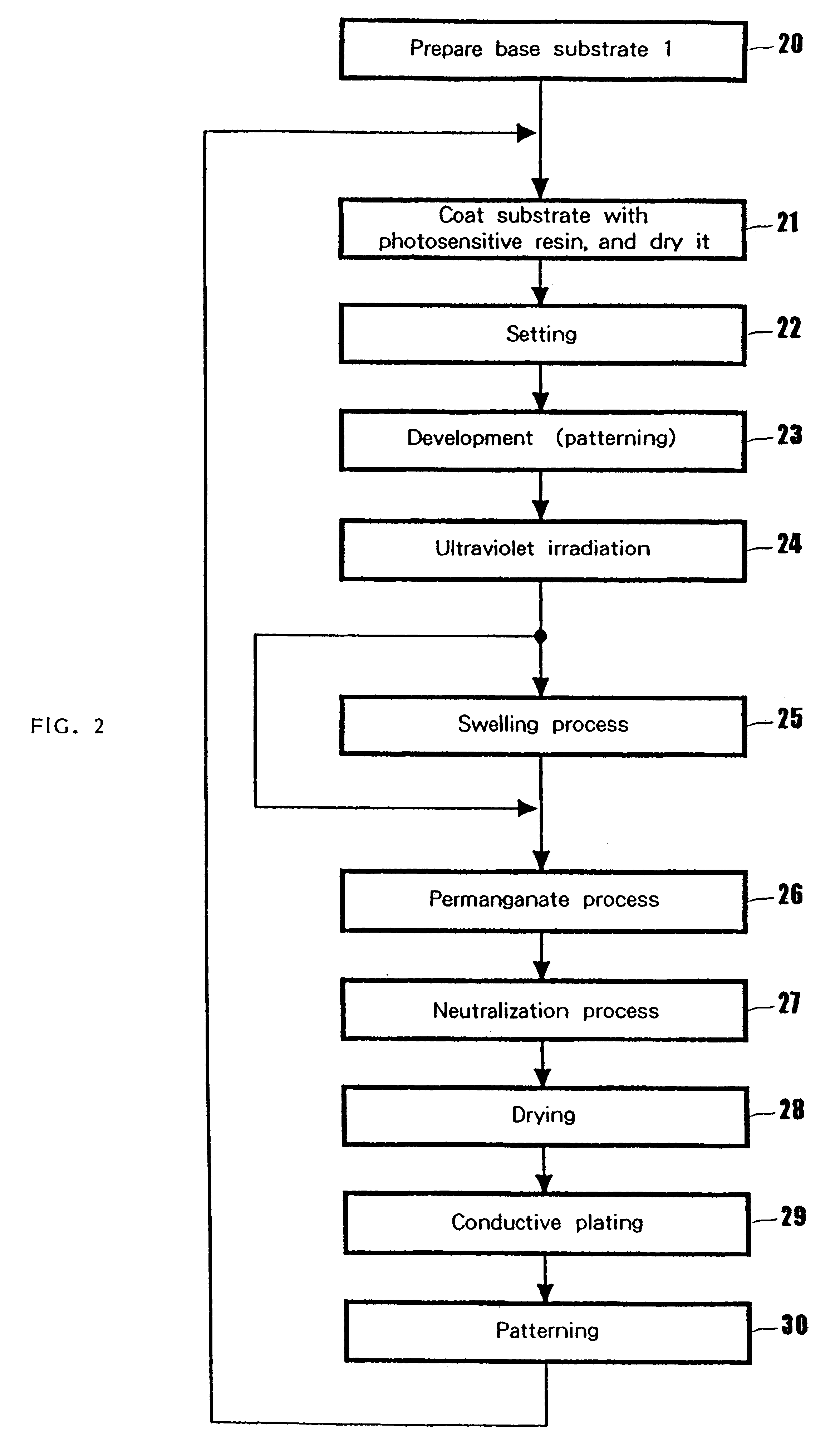
An FR-4 substrate, which is a known glass epoxy resin substrate, both sides of which have copper foil attached, was prepared, and for the substrate, the following process was performed:

(a) A haloless oxidization process was performed on the FR-4 substrate. During this process, copper oxide, which was produced by the pre-copper plating oxidization process, was removed in advance in order to prevent the insulating layer (composed of resin) from peeling off the copper. Specifically, the reduction process was performed after the copper on the surface of the FR-4 substrate had been oxidized, and as a result, to expose the copper foil several angstroms of copper oxide had to be removed from its surface.

(b) The surface of the FR-4 substrate was coated with about 30 .mu.m of photosensitive epoxy resin (Probelec 7136) which was then dried.

(c) The FR-4 substrate was exposed to light using an exposure unit that produced a light quantity of 2000 mJ.

(d) The resultant substrate was heated at 110....


PUM

PropertyMeasurementUnit
peak wavelengthaaaaaaaaaa

Abstract

Methods are provided for the manufacture of a conductive layer on an insulating layer and for the manufacture of a built-up circuit board, each include an innovative step of irradiating the surface of an insulating (resin) layer with ultraviolet light, so that a conventional swelling process can be eliminated or simplified.

Description

The present invention relates to a method for depositing a conductive layer on an insulating layer, and relates more particularly to a method for depositing a conductive layer on an insulating layer for a built-up circuit board.A so-called built-up circuit board is conventionally known as a high-density circuit board wherein an insulating layer and a conductive circuit layer are alternately laminated on a base substrate, on the surface of which a conductive circuit is plated. In the process for manufacturing the built-up circuit board, generally, a conductive (metal) layer is formed on the insulating layer of the base substrate by plating.When the insulating layer is composed of a resin, generally, a pre-process for roughing the surface of the resin layer before metal plating is performed in order to increase the strength of the adhesion between the resin and the plated metal. Oxidization of the surface of the resin layer is one approach and may be performed using an oxidizing agent...

Claims


Application Information

Patent Timeline
Patent Type & Authority Patents(United States)
IPC IPC(8): H05K3/46H05K3/18H05K3/00H05K3/38
CPCH05K3/4661H05K3/0023H05K3/185H05K3/4602Y10T29/49155H05K2203/0796Y10T29/49128Y10T29/49126H05K2201/0959
Inventor SHIRAI, MASAHARU
Owner GLOBALFOUNDRIES US INC
Why Eureka
Try Eureka