Current-controlled CMOS wideband data amplifier circuits

a wideband data and amplifier technology, applied in the field of current-controlled cmos wideband data amplifiers, can solve the problems of inductors needed, limited gain-bandwidth product brought about by such inductive peaking, and not as widely available,

Inactive Publication Date: 2003-09-23
AVAGO TECH INT SALES PTE LTD
View PDF4 Cites 167 Cited by
  • Summary
  • Abstract
  • Description
  • Claims
  • Application Information

AI Technical Summary

Benefits of technology

This invention achieves maximum bandwidth expansion by using series inductor peaking with miller capacitance cancellation technique and shunt inductor peaking in current controlled CMOS circuit (C.sup.3 MOS). The series peaking provides a certain peak bandwidth product depending on the inductance L, the capacitance C, and the quality of these two components. The bandwidth is inversely proportional to the square root of LC. The peaking mainly depends upon the inductance due to its limited Q. By reducing the miller capacitance from the C.sup.3 MOS input a wider bandwidth is obtained with adequate peaking value. The total response of the amplifier can be obtained with wider bandwidth of minimum ripple and minimum phase distortion.

Problems solved by technology

The expansion of the gain-bandwidth product brought about by such inductive peaking, however, is limited to about 1.5 times, and the inductors needed are generally large which requires a large area on an integrated circuit.
However, these technologies are generally more costly and not as widely available as standard CMOS process.

Method used


Image

  • Current-controlled CMOS wideband data amplifier circuits
  • Current-controlled CMOS wideband data amplifier circuits
  • Current-controlled CMOS wideband data amplifier circuits

Examples


Embodiment Construction

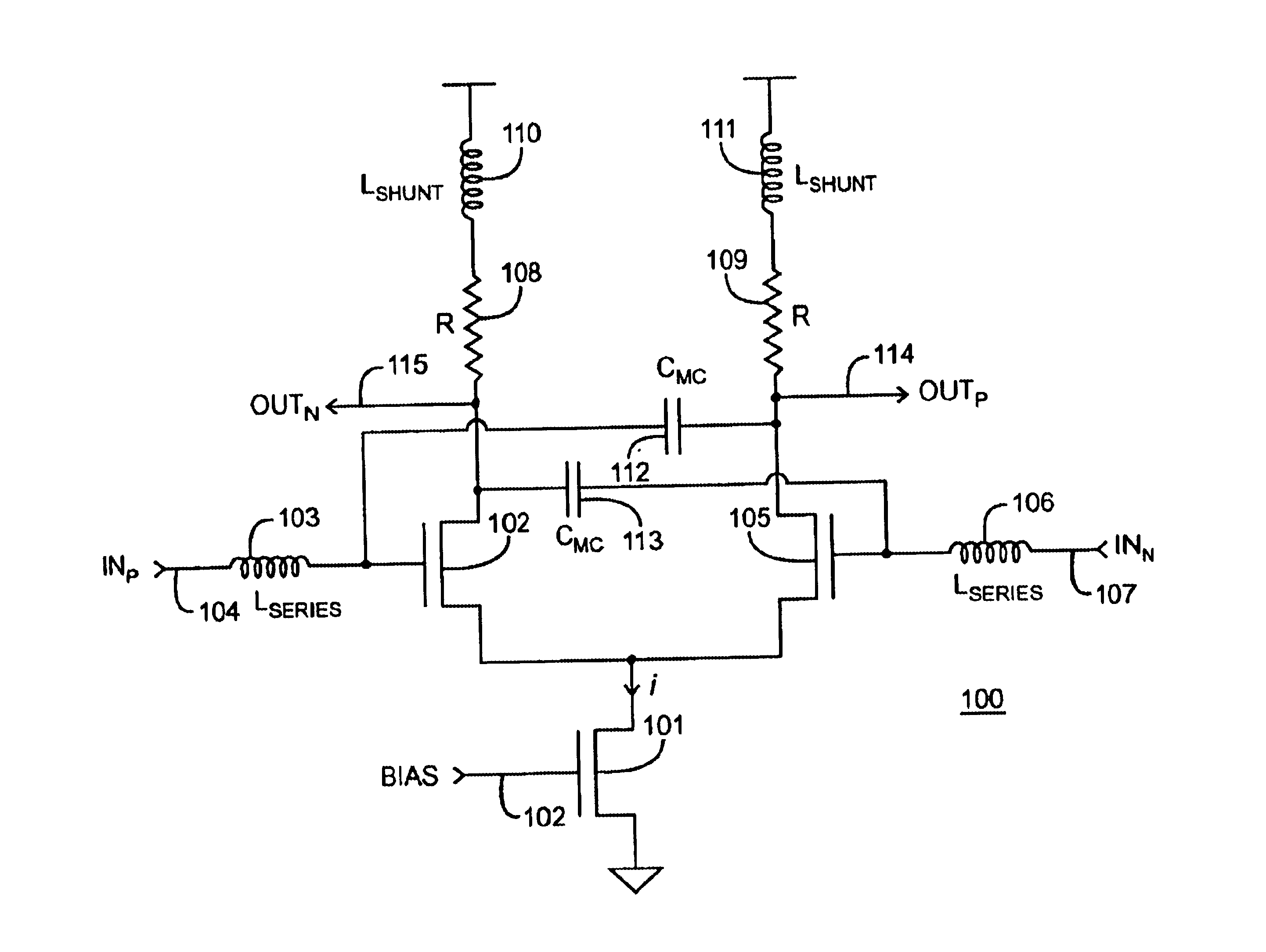
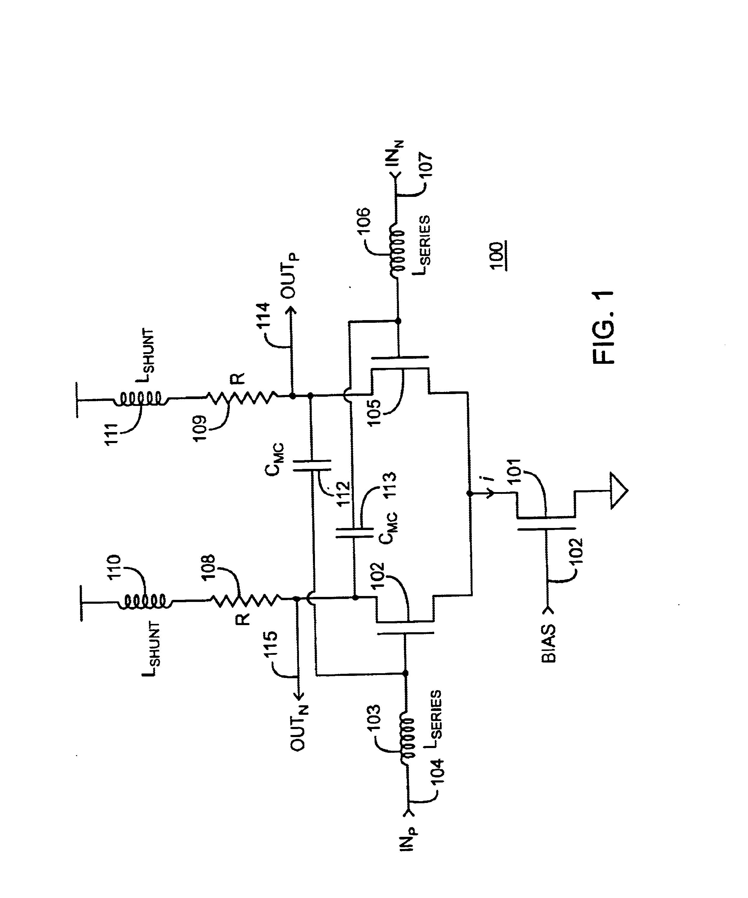
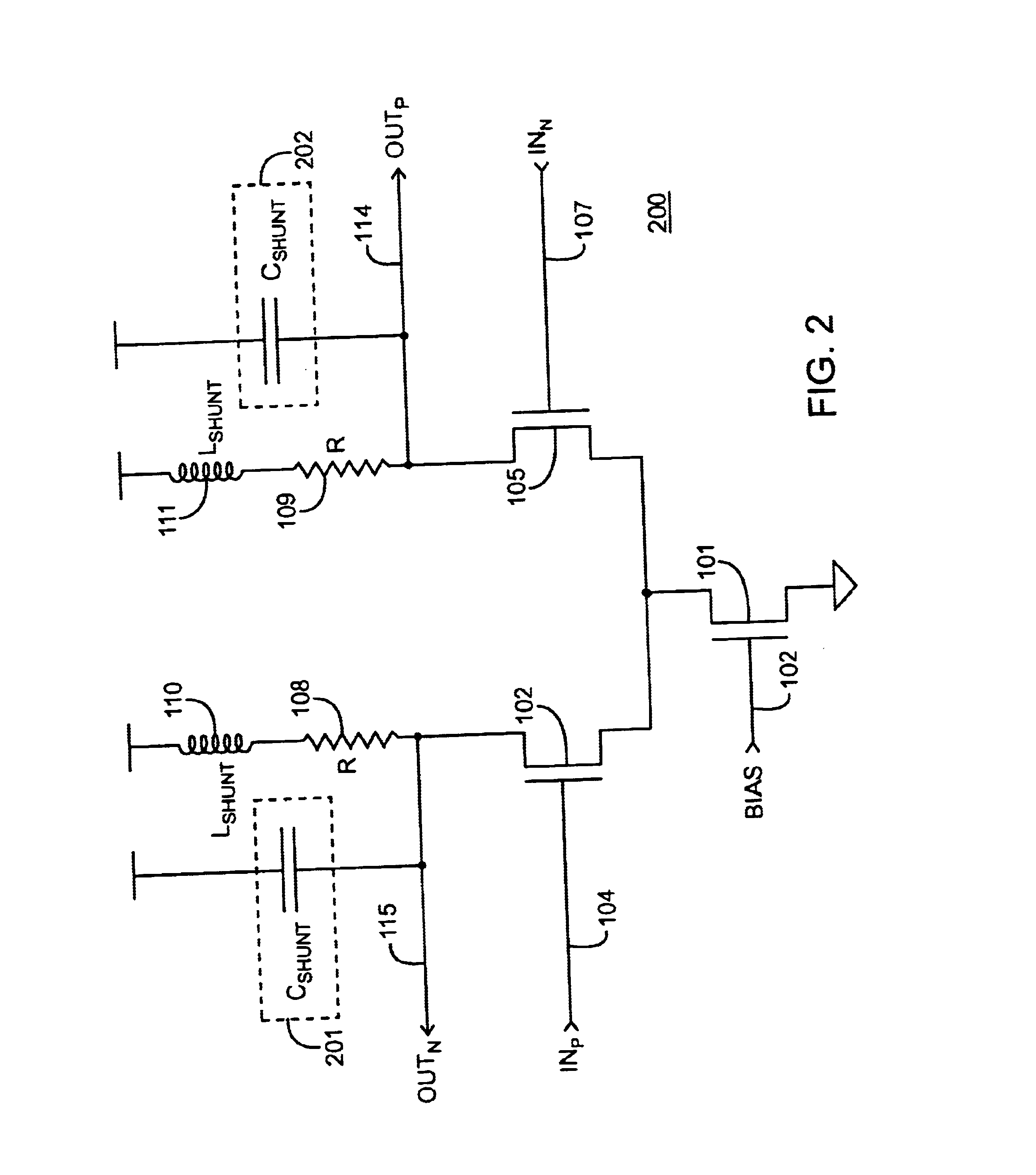
According to an embodiment of the present invention, shunt peaking, and serial peaking are combined in the same wideband data amplifier. In various embodiments of a multi-stage wideband data amplifier, some stages may have serial peaking but not shunt peaking, other stages may have shunt peaking but not serial peaking, other stages may have serial peaking and shunt peaking, and yet other stages may have neither serial peaking nor shunt peaking.

FIG. 1 illustrates an amplifier stage 100 according to one embodiment of the present invention having series peaking, shunt peaking, and miller capacitance cancellation. A current source transistor 101 is biased by a bias voltage so that a constant current i flows from drain to source in the current source transistor 101. A first differential transistor 102 has its gate tied to the negative end of a first series peaking inductor 103, while a positive differential input signal IN.sub.p 104 is coupled to the positive end of the first series peak...


PUM


Abstract

Expansion of the bandwidth of a wideband CMOS data amplifier is accomplished using various combinations of shunt peaking, series peaking, and miller capacitance cancellation. These various combinations are employed in any of the amplifier input stage, in intermediate stages, or in the last stage.

Description

1. Field of the InventionThe present invention pertains to the field of complementary metal-oxide-semiconductor (CMOS) circuitry; and, specifically, to the field of high speed CMOS wideband data amplifiers for wideband data communication applications.2. Discussion of the Related ArtHigh speed wideband data amplifiers are used in wideband data communication applications. For a number of reasons including speed limitations of processing technology, power consumption and other cost related concerns, it is desirable to develop efficient techniques to boost the amplifier bandwidth for higher frequency operations. High speed circuit techniques such as current-controlled CMOS (or C.sup.3 MOS) logic have been developed that have brought about marked increase in the speed of circuitry fabricated using standard CMOS process technology. Various C.sup.3 MOS circuit techniques are described in greater detail in commonly-assigned patent application Ser. No. 09 / 484,856, titled "Current Controlled ...

Claims


Application Information

Patent Timeline
Patent Type & Authority Patents(United States)
IPC IPC(8): H03F1/48H03F1/08H03F1/42H03F1/14
CPCH03F1/14H03F1/483H03F2203/45018H03F2203/45512H03F2203/45554H03F2203/45714
Inventor YIN, GUANGMINGCAO, JUN
Owner AVAGO TECH INT SALES PTE LTD
Why Eureka
Try Eureka