Method and apparatus for a scannable hybrid flip flop

a hybrid flip flop and latch technology, applied in the direction of generating/distributing signals, pulse techniques, instruments, etc., can solve the problems of incompatibility of lssd, circuit disturbance, and modern electronic computer automated design tools, which are directed,

Inactive Publication Date: 2003-09-30
OL SECURITY LIABILITY CO
View PDF23 Cites 27 Cited by
  • Summary
  • Abstract
  • Description
  • Claims
  • Application Information

AI Technical Summary

Problems solved by technology

In a space-based environment, however, ionic strikes by sub-atomic cosmic particles are known to introduce circuit disturbances.
Unfortunately, modern electronic computer automated design (ECAD) tools, which are directed more to automated test pattern generation (ATPG), are incompatible with LSSD.
Unfortunately, an upsetting event occurring in the clock tree prior to clock signal 207 can cause a false clock pulse on clock signal 207.
Additionally, this scan dff 200 is both incompatible with LSSD and is even more sensitive to SEE than LSSD latches.
Furthermore, because an event occurring in the clock tree is, most likely, reflected by errors in chip latches and registers, each clock must be hardened against SEE, which increases clock power requirements and complicates SEE hardening.

Method used


Image

  • Method and apparatus for a scannable hybrid flip flop
  • Method and apparatus for a scannable hybrid flip flop
  • Method and apparatus for a scannable hybrid flip flop

Examples


Embodiment Construction

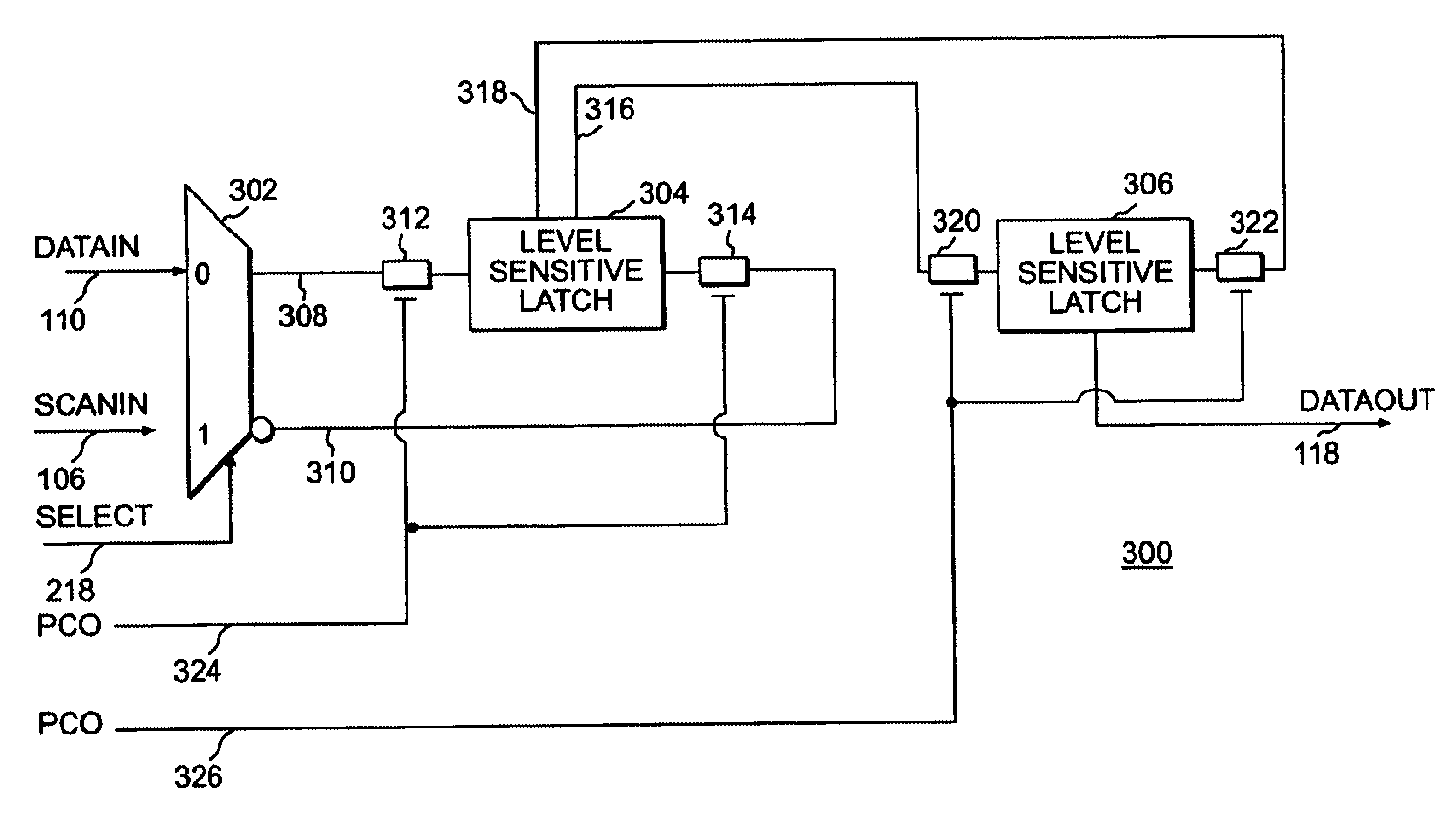
In the following detailed description of illustrative embodiments of the present invention, reference is made to the accompanying drawings which form a part hereof, and in which are shown by way of illustration specific illustrative embodiments in which the invention can be practiced. These embodiments are described in sufficient detail to enable those skilled in the art to practice the invention and it is to be understood that other embodiments can be used and that logical, mechanical and electrical changes can be made without departing from the spirit and scope of the present invention. The following detailed description is, therefore, not to be taken in a limiting sense.

The illustrative embodiments described herein concern electrical circuitry which uses voltage levels to represent binary logic states--namely, a "high" logic level and a "low" logic level. Further, electronic signals used by the various embodiments of the present invention are generally considered active when they...


PUM


Abstract

A scannable flip flop for space-based LSSD testable integrated circuits. A scannable register can be formed from the scannable flip flops. The scannable flip flops can be radiation hardened. Each scannable flip flop can include a 2:1 input multiplexer, a first latch and a second latch. The input multiplexer is coupled to the first latch by a pair of pass gates. The pass gates are gated by a first clock input signal. A second pass gate pair couples the first latch to the second latch. A second clock input signal gates the second pass gate pair. The first and second clock input signals are non-overlapping. The latch can be employed in edge triggered logic ECAD tools for designing IC. The resulting IC logic can be tested using LSSD test testing techniques and patterns.

Description

1. Field of the InventionThe present invention is related to radiation hardened integrated circuits and, more particularly, to scannable latches for radiation hardened integrated circuits.2. Background DescriptionIncreasingly, space-based communication systems are including Integrated Circuits (IC) made in advanced deep sub-micron Field Effect Transistor (FET) technology. Typically, these ICs are in the insulated gate silicon technology commonly referred to as complementary metal oxide semiconductor (CMOS). CMOS ICs are advantageous in that they operate at high speed and use low power, as compared to what other technologies require for comparable speed and function.In a space-based environment, however, ionic strikes by sub-atomic cosmic particles are known to introduce circuit disturbances. These disturbances are known as Single Event Effects (SEEs) and, as Single Event Upsets (SEUs) when occurring in storage elements. Radiation hardened storage elements latches are well known and ...

Claims


Application Information

Patent Timeline
Patent Type & Authority Patents(United States)
IPC IPC(8): G01R31/28G01R31/3185H03K5/15H03K5/151H03K5/1252H03K19/003
CPCG01R31/318552H03K5/1252H03K5/1515H03K19/00338
Inventor HOFFMAN, JOSEPH A.YODER, JOSEPH W.
Owner OL SECURITY LIABILITY CO
Why Eureka
Try Eureka