Microthermistor based fingerprint sensor

a fingerprint sensor and microthermistor technology, applied in image data processing, transmission systems, transmission, etc., can solve the problems of inconvenient use for users, process not providing a good resolution, and time-consuming fingerprint identification activities performed by human operators

Inactive Publication Date: 2003-10-14
INSTITUT NATIONAL D'OPTIQUE
View PDF20 Cites 62 Cited by
  • Summary
  • Abstract
  • Description
  • Claims
  • Application Information

AI Technical Summary

Problems solved by technology

Fingerprint identification can be a time consuming activity when performed by human operators.
This process does not provide a good resolution and is not very convenient for users, as it involves the use of ink on a finger, which is then transferred to a piece of paper.
After having placed the fingerprint on the piece of paper, the user must clean off the ink, which makes the process messy.
Moreover, using these records for fingerprint identification is a very cumbersome and time consuming process.
One operational drawback of this approach is that the optical surfaces in contact with the finger must be cleaned regularly to maintain the system performance.
Moreover, such systems are typically large and the alignment of the various optical components part of the system must be kept within tight tolerances.
The main disadvantage of this approach is that it is very demanding on the membrane properties, as it must be conductive (at least partially), very soft and yet capable of withstanding repeatedly the deformations induced by a user's finger.
This can cause some inaccuracy on the recorded fingerprint feature size and position.
This last system design still allows the grey level representation of fingerprints but has the disadvantages of consuming more energy.
The main drawback of using the thermal conductivity as the parameter for fingerprint recording is that the sensors must be heated and, ideally, this heating should be done separately for each individual sensor.
The problem with this approach is that the charge pattern representing the fingerprint will quickly fade away if the temperature change is not regularly refreshed.
Moreover, it is much more demanding on the sensor response time and on the system data acquisition rate.
The classical approach based on ink and paper has proven to be very unpractical and time consuming.
Other systems based on optical imaging can achieved good performances but they are typically large and require regular maintenance.
The drawback of this method is the required sensor heating and the associated power consumption.
Such pulse heating being inconvenient, other systems rely on fingerprint sweeping across a pyroelectric sensor array which provides the temperature transients necessary for such sensors.
The disadvantages of this solution are that it involves much more complex fingerprint retrieval algorithm and it is much more demanding on the sensor response time and on the system data acquisition rate.

Method used


Image

  • Microthermistor based fingerprint sensor
  • Microthermistor based fingerprint sensor
  • Microthermistor based fingerprint sensor

Examples


Embodiment Construction

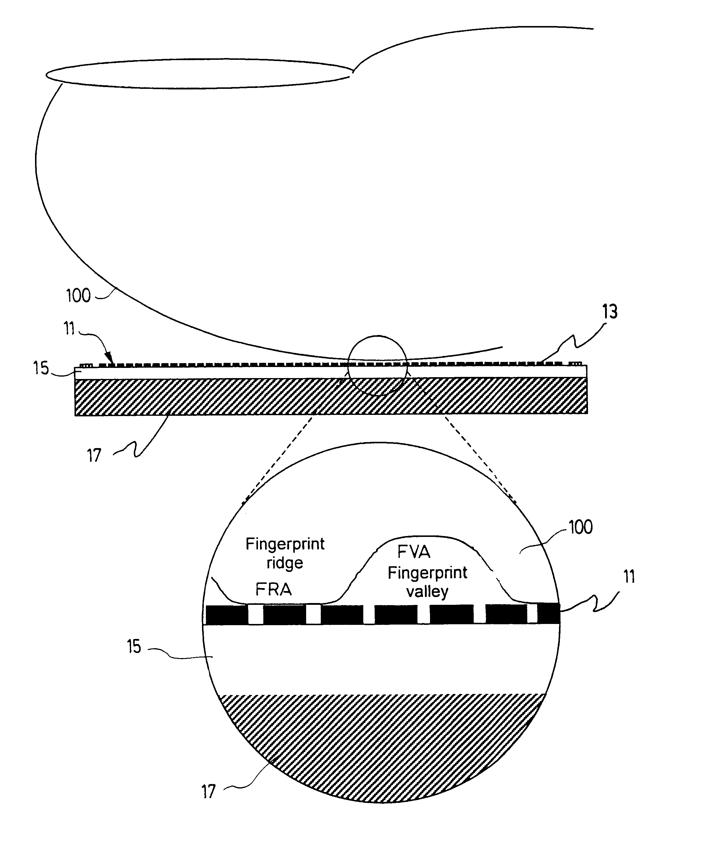
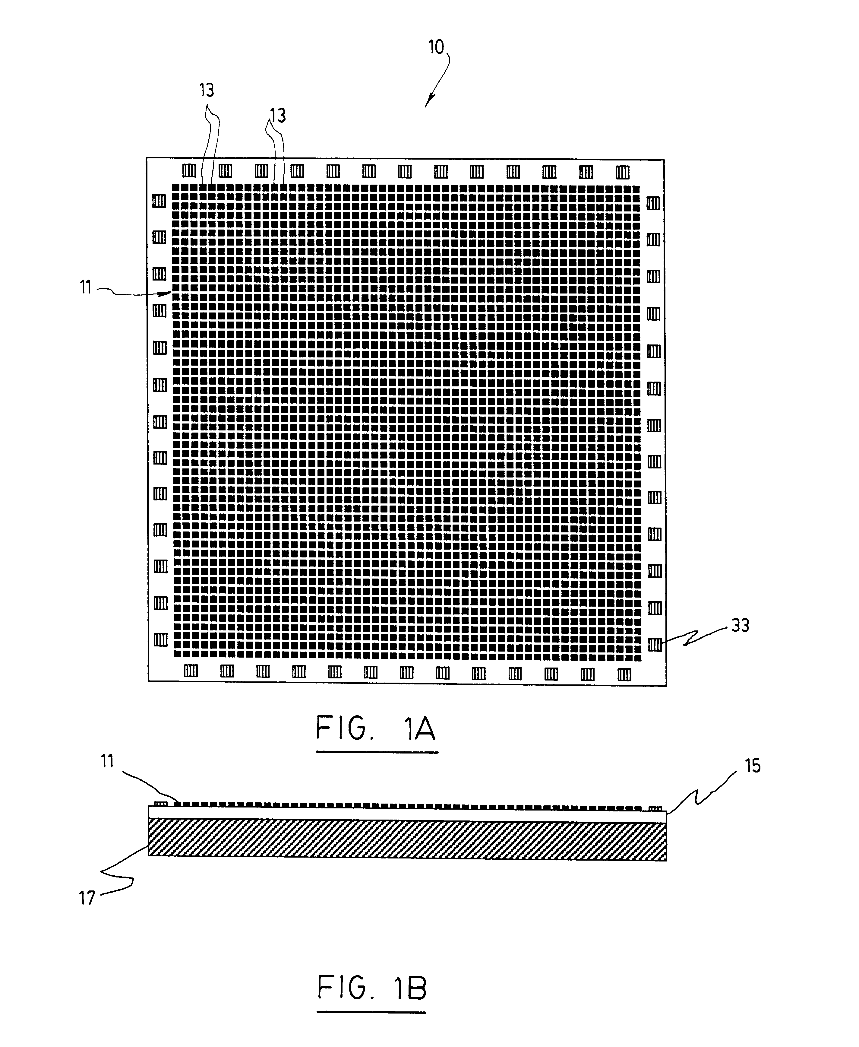
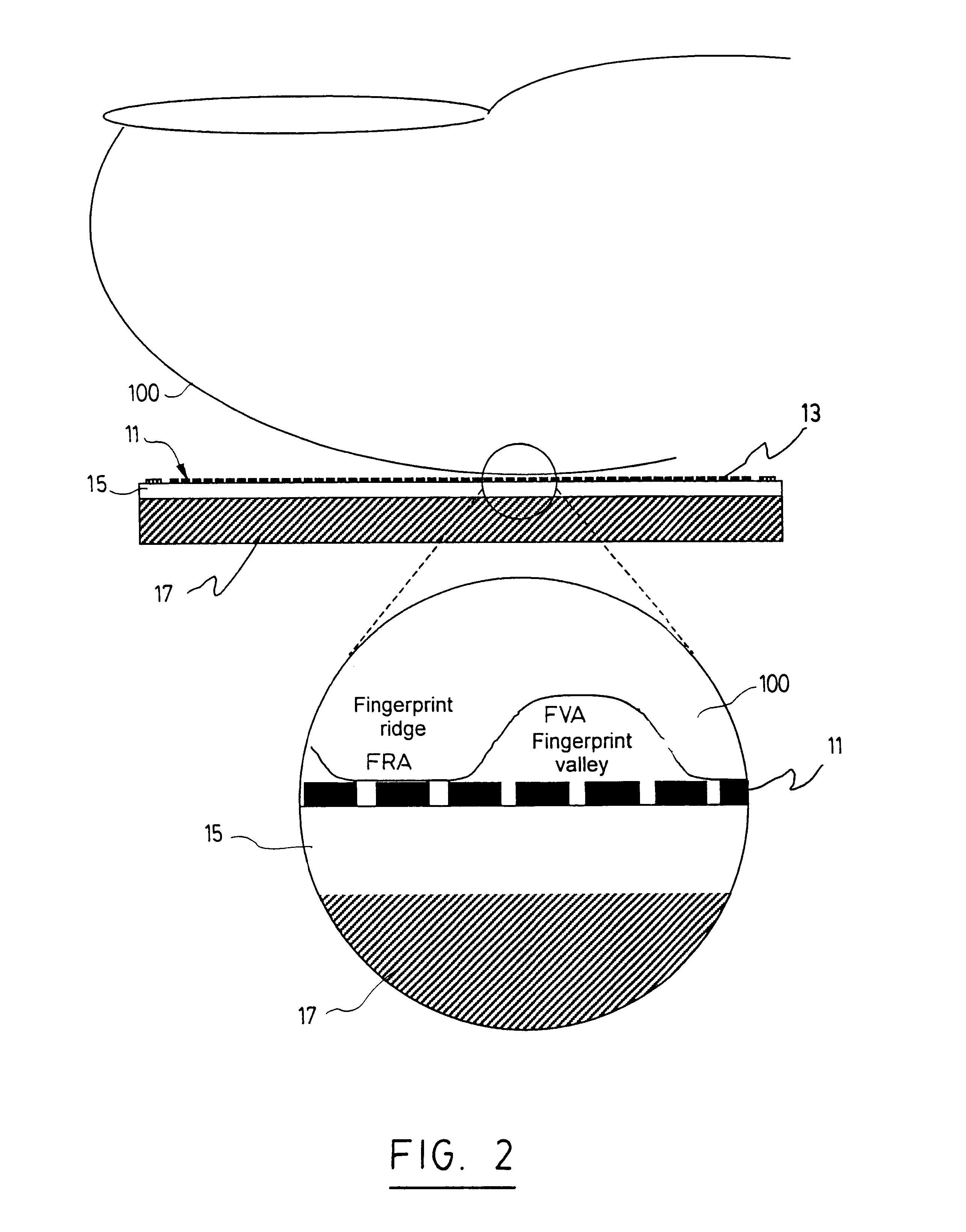
As mentioned previously, the present invention relates to fingerprint sensing, based on a temperature sensing cell array. In broad terms, the fingerprint sensor according to the present invention transforms the ridge and valley pattern of a finger, hereinafter referred to as a fingerprint, into an electronic output signal. Referring now to FIGS. 1a and 1b, the sensor 10 according to the present invention comprises a microthermistor array 11 for converting temperature into an electrical signal, the array 11 being composed of a plurality of microthermistors 13, each of the thermistors 13 being adapted to output an electrical signal proportional to a temperature variation; a read-out integrated circuit 15 operatively connected to the microthermistor array 11 for receiving the electrical signal and converting it into an electronic output signal representative of the ridges and valleys of a finger; and a substrate 17 for supporting the read-out integrated circuit 15 and the microthermist...


PUM

PropertyMeasurementUnit
distanceaaaaaaaaaa
temperatureaaaaaaaaaa
thermalaaaaaaaaaa

Abstract

The present invention concerns a fingerprint sensor which is small; demonstrates high sensitivity, low power consumption, high data acquisition rate and is insensitive to vibration and pressure. The sensor produces a high contrast fingerprint representation and is not subject to repeated deformation which could potentially reduces its lifetime. The fingerprint sensor has a microthermistor array for converting temperature variation into an electrical signal, the array being composed of a plurality of microthermistors, each of the thermistors being adapted to output an electrical signal proportional to a temperature variation; a read-out integrated circuit operatively connected to the microthermistor array for receiving the electrical signal and converting it into an electronic output signal representative of the ridge and valley structure of a finger; and a substrate for supporting the read-out integrated circuit and the microthermistor array. The invention is based on microthermistor array. The ohmic resistance of these sensors varies strongly with temperature. The parameter directly measured in this case is the temperature-induced resistance variation of each individual microthermistor. Signals from each of the microthermistor part of the array represent the fingerprint pattern.</PTEXT>

Description

The present invention relates to a microthermistor based fingerprint sensor.DESCRIPTION OF THE PRIOR ARTFinger tips of human beings exhibit a pattern of ridges and valleys called a fingerprint. This structure is unique to every human being and has long been used for the identification of a person. Of particular interest are the ridge branching and ending points of the structure. These fingerprint features are called minutiae. The position and orientation of the minutiae can be used to characterise a fingerprint and thus minimise the information that has to be stored and processed for identification purposes, while still keeping an accurate fingerprint representation.Fingerprint identification can be a time consuming activity when performed by human operators. This explains why automation of fingerprint identification has received considerable attention. Automated fingerprint identification requires the implementation of two main functions. First, the fingerprint pattern of ridges an...

Claims


Application Information

Patent Timeline
Patent Type & Authority Patents(United States)
IPC IPC(8): G01K17/00G06K9/00
CPCG06K9/0002G01K17/003G06V40/1306
Inventor PICARD, FRANCIS
Owner INSTITUT NATIONAL D'OPTIQUE
Why Eureka
Try Eureka