Optical information processing equipment and semiconductor light emitting device suitable therefor

a technology of optical recording equipment and light emitting device, which is applied in the direction of semiconductor devices, lasers, semiconductor lasers, etc., can solve the problems of high operational current density, insufficient characteristics, and inability to achieve the effect of optical recording equipment capable of processing dynamic images of high-definition tvs

Inactive Publication Date: 2003-10-28
USHIO OPTO SEMICON
View PDF12 Cites 278 Cited by
  • Summary
  • Abstract
  • Description
  • Claims
  • Application Information

AI Technical Summary

Problems solved by technology

However, there has yet to be realized an optical recording equipment capable of sufficiently processing dynamic images of high-definition TVs.
In recent years, continuous oscillation at room temperature of a semiconductor laser device using an undoped InGaN quantum-well layer provided on a sapphire substrate as a light emitting layer has been realized (S. Nakamura et al., Appl. Phys. Lett. 69 (1996) 4056) This semiconductor laser device, however, has required a high operational current density, thereby failing to obtain sufficient characteristics from the viewpoint of practical use.
This semiconductor laser device, however, has also required a high operational current density, thereby failing to realize continuous oscillation thereof.

Method used


Image

  • Optical information processing equipment and semiconductor light emitting device suitable therefor
  • Optical information processing equipment and semiconductor light emitting device suitable therefor
  • Optical information processing equipment and semiconductor light emitting device suitable therefor

Examples


second example

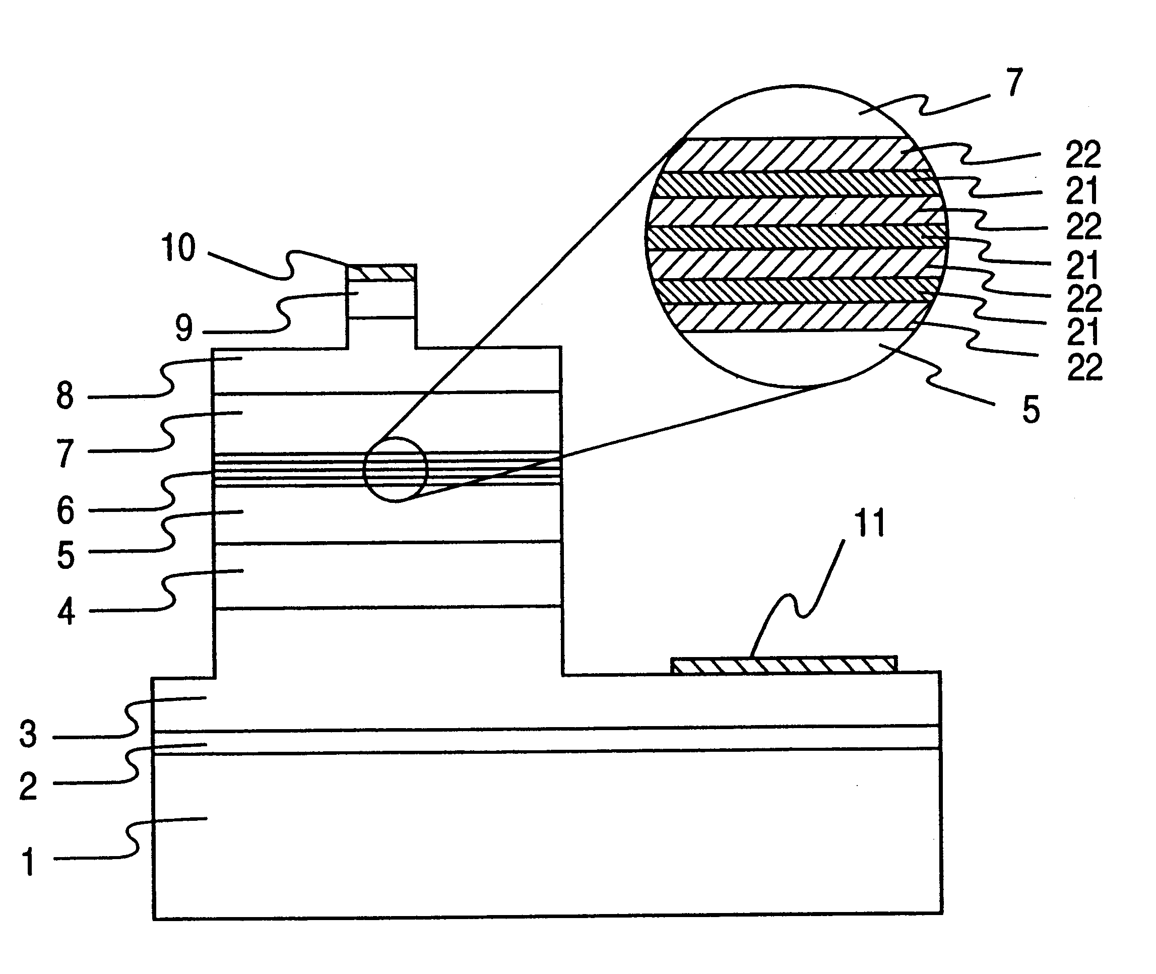
A semiconductor laser device in this example of the present invention will be described with reference, also, to FIG. 14.

The semiconductor laser device having a multi-quantum well structure in this example is formed by sequentially stacking, on a sapphire substrate 1 with the (1,0,-1,2) plane taken as the principle plane thereof, a low temperature buffer layer 2 made from n-type GaN, a high temperature buffer layer 3 made from n-type GaN, an n-type Al.sub.0.2 Ga.sub.0.8 N cladding layer 4, an n-type GaN optical guide layer 5, a GaInN multi-quantum well active region 6, a p-type GaN optical guide layer 7, a p-type Al.sub.0.2 Ga.sub.0.8 N cladding layer 8, and a p-type GaN cap layer 9. Each of these layers is formed by epitaxial growth by the usual metal organic vapor phase epitaxial growth method. The thickness of each layer is set at 0.05 .mu.m (low temperature buffer layer 2), 3 .mu.m (high temperature buffer layer 3), 0.3 .mu.m (n-type cladding layer 4), 0.1 .mu.m (n-type optical ...

third example

FIG. 15 is a structural sectional view, taken from a plane crossing an optical axis, showing a semiconductor laser device as a third example of the present invention.

The semiconductor laser device having a multi-quantum well structure in this example is formed by sequentially stacking, on an n-type SiC substrate 51 with the (1,0,-1,0) plane taken as the principle plane thereof, a low temperature buffer layer 2 made from n-type GaN, a high temperature buffer layer 3 made from n-type GaN, an n-type Al.sub.0.2 Ga.sub.0.8 N cladding layer 4, an n-type GaN optical guide layer 5, a GaInN multi-quantum well active region 6, a p-type GaN optical guide layer 7, a p-type Al.sub.0.2 Ga.sub.0.8 N cladding layer 8, and a p-type GaN cap layer 9. Each of these layers (and region) is formed by epitaxial growth by the usual metal organic vapor phase epitaxial growth method. The thickness of each layer is set at 0.05 .mu.m (low temperature buffer layer 2), 3 .mu.m (high temperature buffer layer 3), 0...

fourth example

A semiconductor laser device in this embodiment will be described with reference to FIG. 14.

The semiconductor laser device having a multi-quantum well structure in this example is formed by sequentially stacking, on a sapphire substrate 1 with the (1,0,-1,2) plane taken as the principle plane thereof, a low temperature buffer layer 2 made from n-type AlN, a high temperature buffer layer 3 made from n-type AlN, an n-type Al.sub.0.2 Ga.sub.0.8 N cladding layer 4, an n-type GaN optical guide layer 5, a GaInN multi-quantum well active region 6, a p-type GaN optical guide layer 7, a p-type Al.sub.0.2 Ga.sub.0.8 N cladding layer 8, and a p-type GaN cap layer 9. Each of these layers is formed by epitaxial growth by the usual metal organic vapor phase epitaxial growth method. The thickness of each layer is set at 0.05 .mu.m (low temperature buffer layer 2), 3 .mu.m (high temperature buffer layer 3 ), 0.3 .mu.m (n-type cladding layer 4 ), 0.1 .mu.m (n-type optical guide layer 5 ), 0.1 .mu.m ...


PUM


Abstract

An information processor of a high reliability and a high recording density, and a blue color, blue-violet color and violet color based semiconductor light emitting device operable at a low threshold current density, used for the same, are provided. An optical information processor of a high reliability and a high recording density enables a moving picture, such as a high-definition television picture, to be recorded and reproduced satisfactorily. A barrier layer in a quantum-well active layer of a semiconductor light emitting device is doped with n-type impurities at a high density. Alternatively, the face orientation of a quantum-well active layer of a semiconductor light emitting device is a plane inclined from the (0001) plane, whereby the threshold current value of the semiconductor light emitting device can be decreased. The semiconductor light emitting device is typified by a gallium nitride based compound semiconductor laser device.

Description

The present invention relates to optical information processing equipment such as an optical disk apparatus and a light source, particularly, a semiconductor light emitting device suitable therefor.With regard to optical information processing equipment represented by a DVD (Digital Video Disk) apparatus, there have been strong demands to increase the capacity thereof. In particular, it has been required to provide optical information processing equipment capable of processing images of high-definition TVs. As such information processing equipment, there has been generally known a type adopting a photomagnetic recording or phase transition recording method. However, there has yet to be realized an optical recording equipment capable of sufficiently processing dynamic images of high-definition TVs.On the other hand, with regard to a semiconductor light emitting device used as a light source of such optical information equipment, it has been required to shorten the wavelength toward a...

Claims


Application Information

Patent Timeline
Patent Type & Authority Patents(United States)
IPC IPC(8): H01S5/343H01S5/00H01S5/32H01S5/34
CPCB82Y20/00H01S5/34333H01S5/343H01S5/3202H01S5/3407H01S5/320275
Inventor NIWA, ATSUKOOHTOSHI, TSUKURUKURODA, TAKAOOKAI, MAKOTOSHIMANO, TAKESHI
Owner USHIO OPTO SEMICON
Why Eureka
Try Eureka