Double-side polishing process with reduced scratch rate and device for carrying out the process

a technology of polishing process and chip, which is applied in the direction of grinding machine, manufacturing tool, lapping machine, etc., can solve the problems of crystallite formation, scratches on the polished semiconductor wafer, and insufficient conventional single-side polishing process to produce semiconductor wafers

Inactive Publication Date: 2003-11-11
SILTRONIC AG
View PDF20 Cites 16 Cited by
  • Summary
  • Abstract
  • Description
  • Claims
  • Application Information

AI Technical Summary

Benefits of technology

An essential feature of the invention is that, by preventing the polishing abrasive supplied from drying out, crystallization of the colloid, which leads to scratches being formed on the surfaces of the semiconductor wafers, is avoided. The fact that only the combination of the measures of (a) wetting of the outer and / or inner gear teeth of the polishing machine and (b) using a closed polishing-abrasive supply, which prevent the polishing abrasive from drying out, considerably reduces the scratch rate on the semiconductor wafers. This is unexpectedly surprising and was impossible to predict.
The carriers are in contact with the polishing machine, for example by means of a pin wheel gear or an involute gear, via a rotating inner drive pin or gear ring and an outer drive pin or gear ring, which generally rotates in the opposite direction. As a result they are set in rotary motion between the two polishing plates. On account of the relative simplicity of exchanging pins which become worn through the constant action of the carrier flanks, the pin gear is preferred within the context of the invention in order to reduce the number of scratches. A further reason is that because of the optimized transmission of forces between the semicircular cutout of the carrier gear and the drive pins, which is optimized compared to that achieved with the sawtooth-like involute gear, the machine operates with fewer vibrations. Also it is therefore possible, by quicker rotation kinetics and a higher pressure, to achieve more advantageous material-removal rates during polishing, for example 0.8 to 1.5 mm / min. Drive pins which comprise a fixedly mounted pin and an exchangeable, secured, yet freely rotatable sleeve pushed over the pin, made from hardened VA steel, are particularly preferred.
The double-side polishing process according to the invention makes it possible to produce semiconductor wafers from silicon which satisfy the requirements for the fabrication of modern semiconductor components. In this process, when large quantities of wafers are produced, a reject rate caused by scratches of only 0.5 to 2% is observed if double-sided polishing is carried out with spraying of the outer and / or inner drive gear ring and with a closed supply of polishing abrasive. This leads to cost savings over processes of the prior art. A process according to the prior art without the inventive features, by contrast, leads to a scrap rate caused by scratches which is of the order of magnitude of 5% to 20%. This leads to higher production costs, for example through the need to reject the wafers or for complex further polishing without the guarantee of success and with the risk of an adverse effect on other quality parameters.

Problems solved by technology

Conventional single-side polishing processes are no longer sufficient to produce semiconductor wafers which satisfy increasingly stringent geometry and nano-topography requirements.
However, different factors of influence, for example coagulation, and as a result crystallization of the polishing abrasive cause crystallites to form in the open supply under the action of ambient air.
In addition, abrasion of polishing-abrasive deposits and extremely small metal particles can be formed on the drive gears and constantly cause scratches on the polished semiconductor wafers.
These scratches can only be removed to a certain extent by expensive further polishing and lead to increased levels of scrap.
In the case of double-side polishing, the use of this process has had only limited success, since there is a continuous supply of particles from the polishing-abrasive ring channel and / or from the gears.
Manual cleaning of these components generally only provides a remedy for a short time.
Although this process reduces the risk of scratches being formed by metal particles, it has no effect on the formation of scratches caused by encrusted polishing abrasive flaking or being rubbed off.
The prior art has not hitherto disclosed any process for the double-side polishing of semiconductor wafers which ensures a constantly low scratch rate.
This is unexpectedly surprising and was impossible to predict.
This prevents the crystallites from being carried between the upper and lower polishing plates, so that they could cause scratches on the silicon wafers.
A design of this type is complex, since the polishing abrasive from the feed line, in the unmoving central part of the polishing machine, can only be transferred into the ring channel by rotary passages of complicated design.
This leads to higher production costs, for example through the need to reject the wafers or for complex further polishing without the guarantee of success and with the risk of an adverse effect on other quality parameters.

Method used


Image

  • Double-side polishing process with reduced scratch rate and device for carrying out the process
  • Double-side polishing process with reduced scratch rate and device for carrying out the process
  • Double-side polishing process with reduced scratch rate and device for carrying out the process

Examples


Embodiment Construction

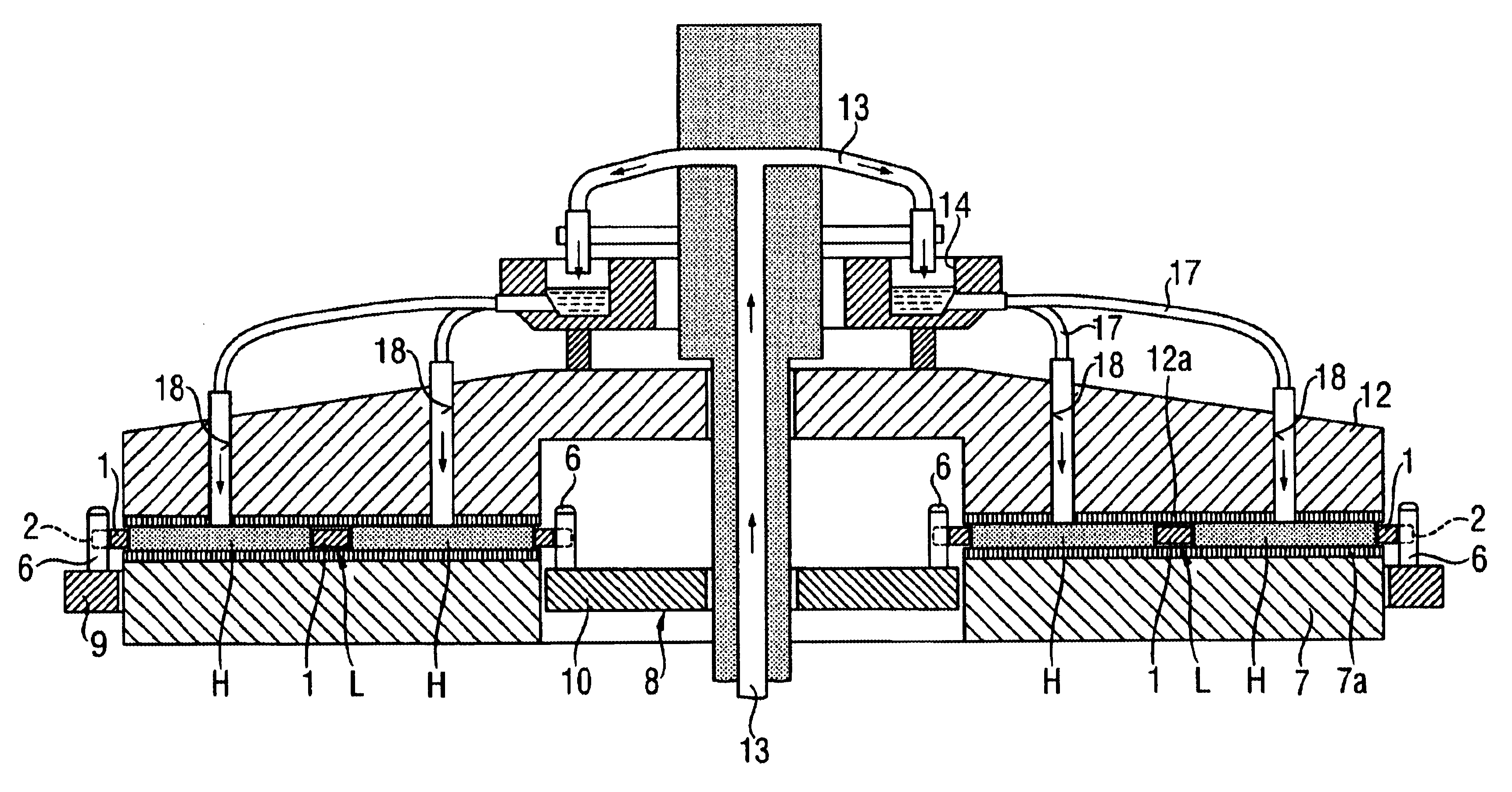
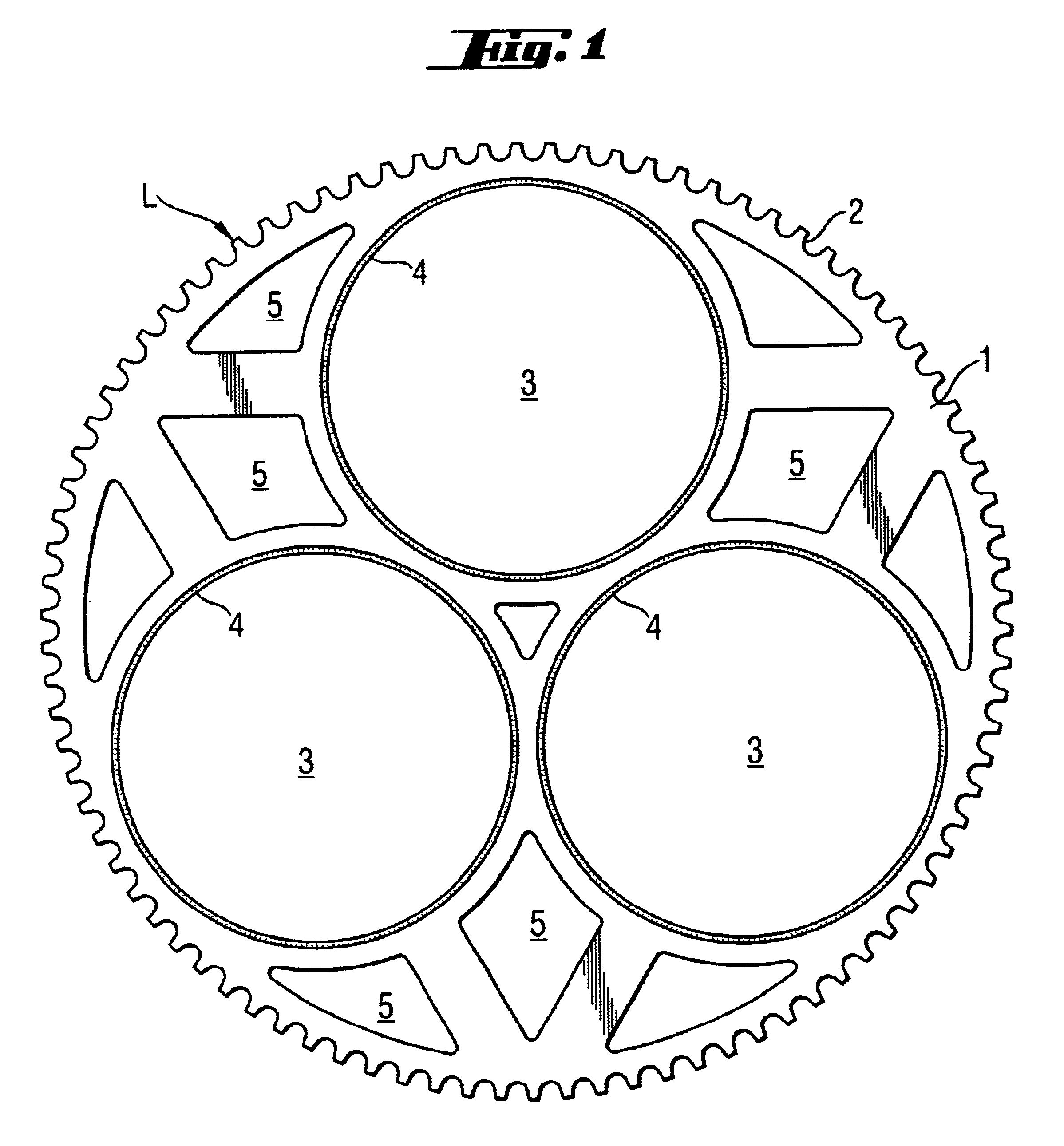
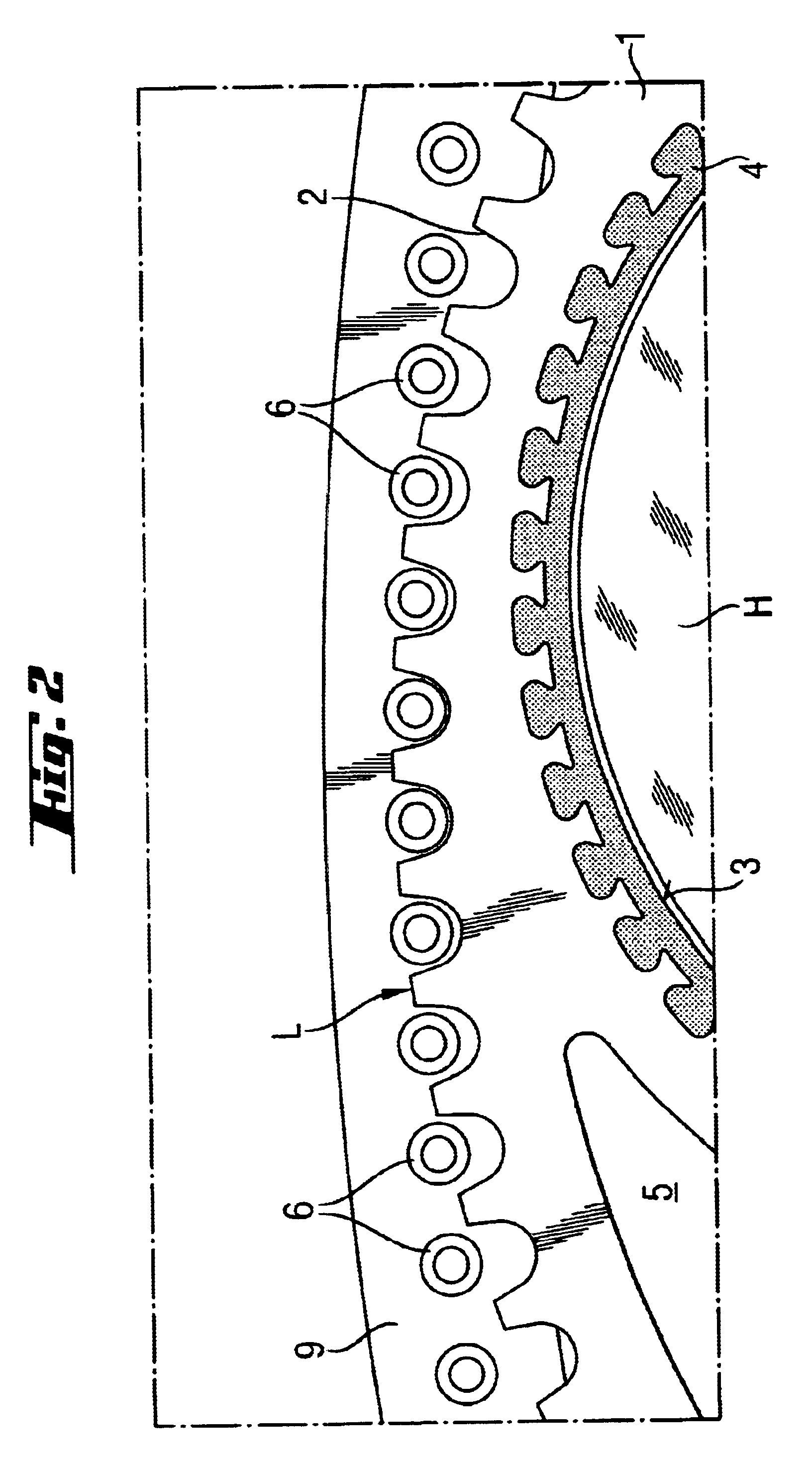
Silicon wafers which had been edge-rounded, ground (removal of silicon 90 .mu.m) and acid-etched in a mixture of concentrated nitric acid and hydrofluoric acid (silicon removal 20 .mu.m), with a diameter of 300 mm and a thickness of 805 .mu.m were available on a production scale for the Example and the Comparative Example. In addition, there were five carriers as shown in FIG. 1. The carriers L comprised a polished metal body 1 made from stainless chromium steel with a mean thickness of 770 .mu.m, which had a circumferential ring gear 2 comprising semicircular cutouts, with which, as shown in FIG. 2, pins 6 of the outer and inner drive pin wheel of a double-side polishing machine engage, so that the carriers can be set in rotation. In each case three circular cutouts 3 which are arrange at regular intervals over a circular path were lined with frames 4 of polyvinylidene difluoride, which had an internal diameter of 301 mm and were of the same thickness as the carrier 1, were connect...


PUM

PropertyMeasurementUnit
diametersaaaaaaaaaa
diametersaaaaaaaaaa
diametersaaaaaaaaaa

Abstract

A process for producing semiconductor wafers by double-sided polishing between two rotating, upper and lower polishing plates, which are covered with polishing cloth, while an alkaline polishing abrasive with colloidal solid fractions is being supplied, the semiconductor wafers being guided by carriers which have circumferential gear teeth and are set in rotation by complementary outer gear teeth and inner gear teeth of the polishing machine, which is distinguished by the following process steps:(a) at least one of the two sets of gear teeth of the polishing machine is at least from time to time sprayed with a liquid which substantially comprises water,(b) the alkaline polishing abrasive is fed continuously to the semiconductor wafers in a closed supply device. There is also a device which is suitable for carrying out the process.

Description

1. Field of the InventionThe present invention relates to a double-side polishing process for semiconductor wafers, which are used in particular in industry for the fabrication of microelectronic components. The invention also relates to a device which is suitable for carrying out the process.2. The Prior ArtTechnological progress in the fabrication of microelectronic components, for example processors and memory components, requires the provision of single-crystal semiconductor wafers as a platform. These wafers have to satisfy increasingly stringent specifications. Specifications of this type relate to the crystal quality, and relate to the surface, in particular the front surface which is intended for component fabrication, and relate to the geometry and to the nano-topography of wafers of this type.Conventional single-side polishing processes are no longer sufficient to produce semiconductor wafers which satisfy increasingly stringent geometry and nano-topography requirements. M...

Claims


Application Information

Patent Timeline
Patent Type & Authority Patents(United States)
IPC IPC(8): B24B37/04H01L21/02H01L21/306B24B37/005B24B55/06B24B37/08H01L21/304
CPCB24B37/0056H01L21/02024B24B37/08
Inventor WENSKI, GUIDOGLAS, JOHANNALTMANN, THOMASHEIER, GERHARD
Owner SILTRONIC AG
Why Eureka
Try Eureka