High resist-selectivity etch for silicon trench etch applications

a trench etch and high resist-selectivity technology, applied in the direction of basic electric elements, semiconductor/solid-state device manufacturing, electric devices, etc., can solve the problems of high volume devices, undesirable associated costs, and high cost of low cost (and hence low margin)

Inactive Publication Date: 2003-11-25
APPLIED MATERIALS INC
View PDF16 Cites 14 Cited by
  • Summary
  • Abstract
  • Description
  • Claims
  • Application Information

AI Technical Summary

Benefits of technology

Another advantage of the present invention is that trenches can be formed with good profile control.
Yet another advantage of the present invention is that chamber deposits are reduced relative to traditional HBr / Cl.sub.2 chemistry, due to the fluorine-based chemistry of the present invention. Hence, MWBC values are increased.

Problems solved by technology

As a result, relative to processes in which trenches are directly defined with a photoresist mask, an additional oxide-etching step is required to define the mask, and the associated cost is undesirable for low cost (and hence low margin) and high volume devices.
However, traditional silicon / polysilicon etch chemistry is typically based on HBr / Cl.sub.2 chemistry, which has its own limitations.

Method used


Image

  • High resist-selectivity etch for silicon trench etch applications
  • High resist-selectivity etch for silicon trench etch applications
  • High resist-selectivity etch for silicon trench etch applications

Examples


Embodiment Construction

As a preface to the detailed description, it should be noted that, as used in this specification and the appended claims, the singular forms "a", "an", and "the" include plural referents, unless the context clearly dictates otherwise.

All percentages (%) listed for gas constituents are % by volume, and all ratios listed for gas constituents are volume ratios.

The term "selectivity" is used to refer to a) a ratio of etch rates of two or more materials and b) a condition achieved during etch when etch rate of one material is increased in comparison with another material.

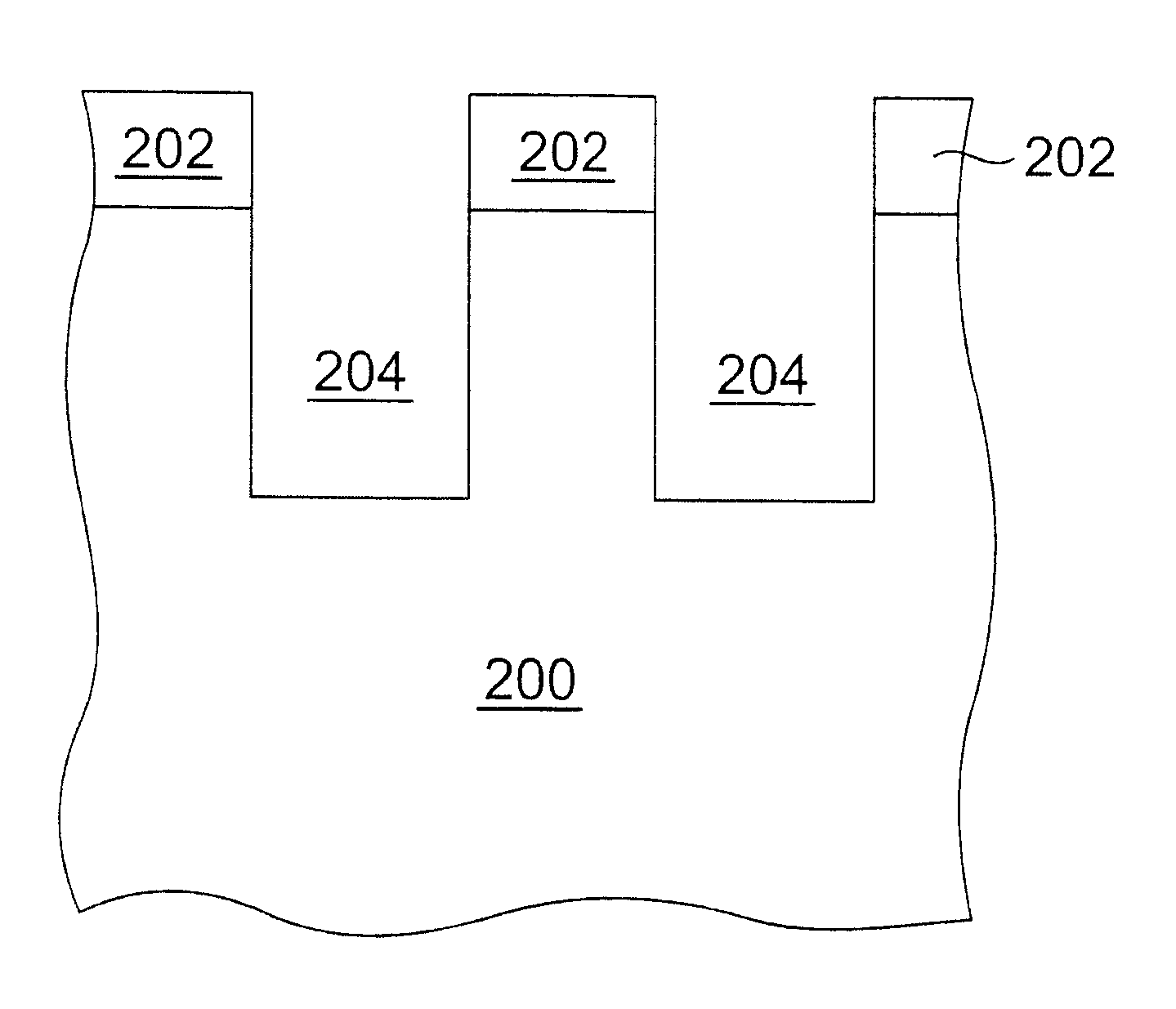
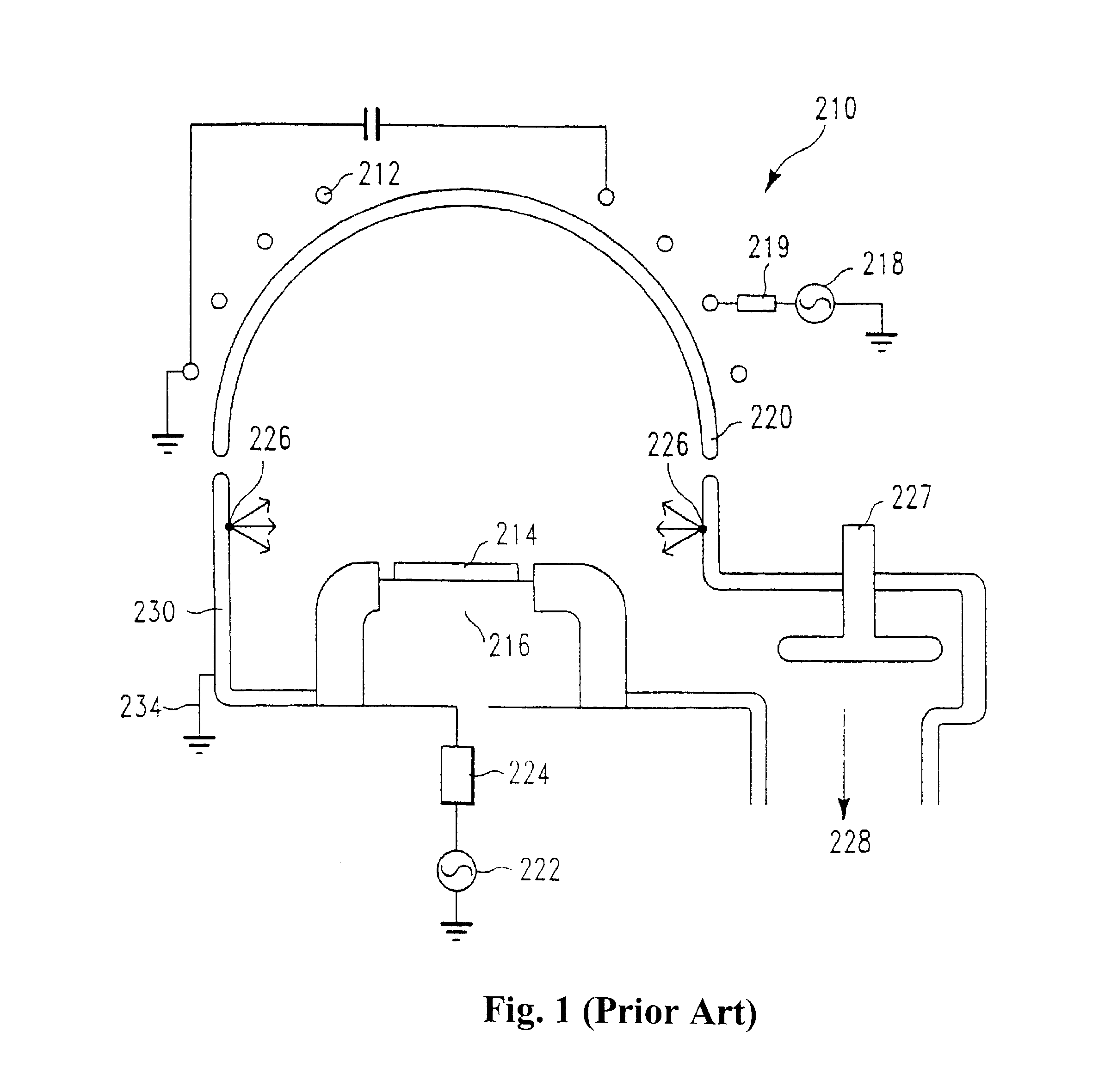
Preferably, etching is carried out in a DPS (decoupled plasma source) etching system. However, it should be appreciated that other inductively coupled plasma sources can be used. Such plasma sources are capable of producing high-density plasmas (e.g., ion densities of 10.sup.11 to 10.sup.12 cm.sup.-3).

A schematic diagram of one such system, which is disclosed in U.S. Pat. No. 6,074,954, the entire disclosure of which is ...


PUM


Abstract

Processes for forming trenches within silicon substrates are described. According to an embodiment of the invention, a masked substrate is initially provided that comprises (a) a silicon substrate and (b) a patterned resist layer over the silicon substrate. The patterned resist layer has one or more apertures formed therein. Subsequently, a trench is formed in the substrate through the apertures in the resist layer by an inductive plasma-etching step, which is conducted using plasma source gases that comprise SF6, at least one fluorocarbon gas, and N2. If desired, Cl2 can also be provided in addition to the above source gases. The process of the present invention produces chamber deposits in low amounts, while providing high etching rates, high silicon:resist selectivities, and good trench sidewall profile control.

Description

1. Field of the InventionThe present invention relates to methods of etching trenches in silicon, and more particularly to methods of etching trenches in silicon while maintaining good photoresist selectivity.2. Brief Description of the Background ArtA number of semiconductor devices, including optical waveguides, optical switches and MOSFET (metal oxide semiconductor field effect transistor) devices require the formation of silicon trenches at some point in their fabrication. Depending on the application, trench depths typically range from 1 to 4 microns in width and 0.5 to 5 in depth, although depths and widths beyond these ranges are clearly possible. In order to etch such silicon trenches, either a photoresist mask or an oxide hard-mask is typically used.The use of an oxide hard-mask in the process integration sequence is presently preferred, because silicon etching at high etch rates, along with high selectivity relative to the oxide mask, is readily achieved using halogen-base...

Claims


Application Information

Patent Timeline
Patent Type & Authority Patents(United States)
IPC IPC(8): H01L21/02H01L21/3213H01L21/3065
CPCH01L21/32137H01L21/3065
Inventor DESHMUKH, SHASHANKMUI, DAVIDCHINN, JEFFREY D.PODLESNIK, DRAGAN V
Owner APPLIED MATERIALS INC
Why Eureka
Try Eureka