
Multimode planar spectrographs for wavelength demultiplexing and methods of fabrication

Inactive Publication Date: 2003-12-02
IBM CORP
View PDF14 Cites 114 Cited by
  • Summary
  • Abstract
  • Description
  • Claims
  • Application Information

AI Technical Summary

Problems solved by technology

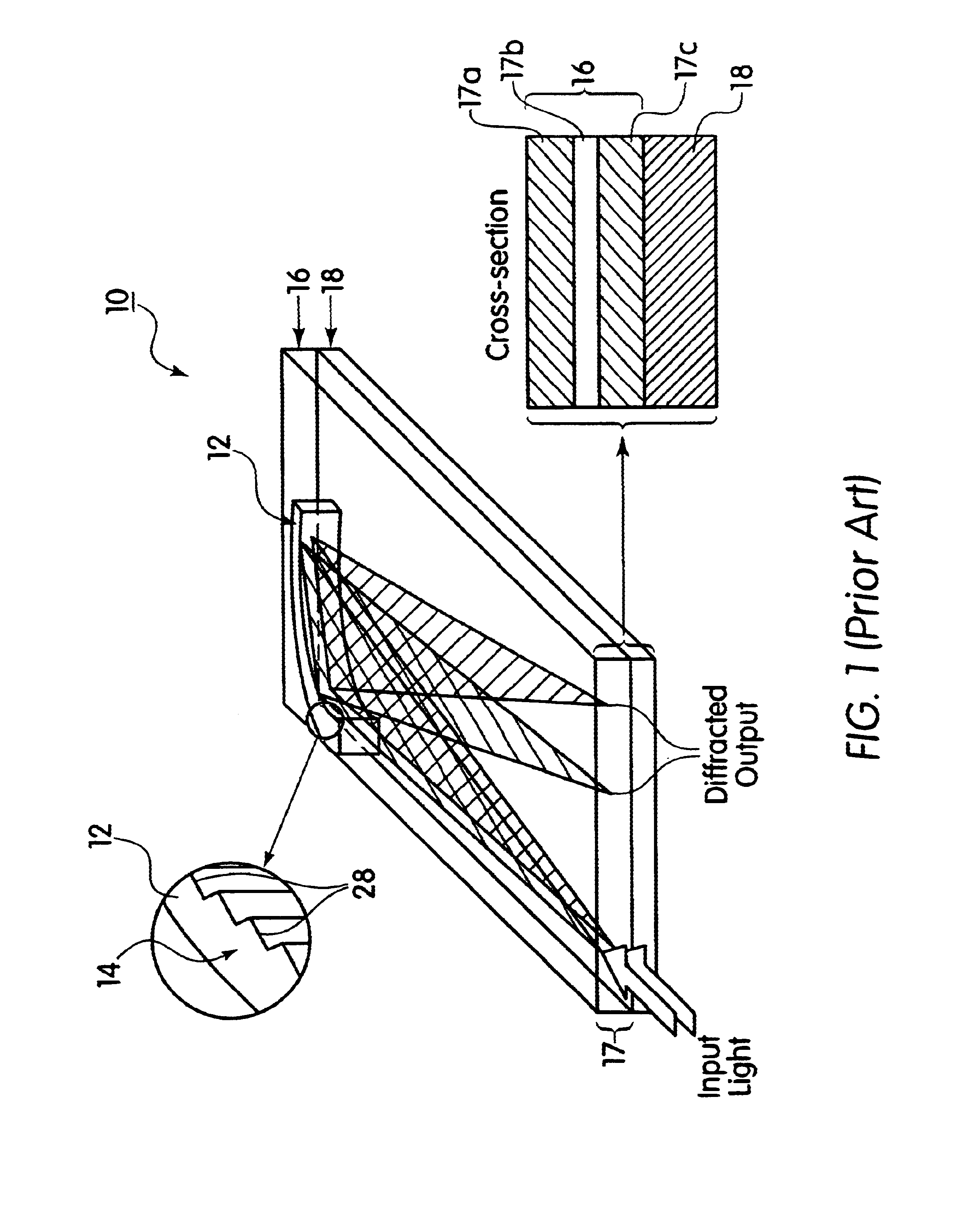
Depositing and etching glass layers 17 to form a MMF-compatible planar spectrograph in a manner similar to that for the single-mode device are no longer practically or technically feasible for glass slab waveguide layers of these thicknesses.
These approaches suffer from several drawbacks and difficulties with respect to their ultimate levels of performance and their ability to be packaged.
Since continual adjustment between successive scribes would be laborious, time-consuming, and expensive, the grating pitch and blaze are normally changed step-wise for only a few segments of the length of a ruled grating.
Furthermore, blazing of holographic grating facets is limited.
Relative misalignments may occur and are an additional source of concern for aberrations in the output images.
Polymers, however, are generally frowned upon for use in LAN datacom transceivers due to their uptake of moisture in non-hermetic packaging, high sensitivity to operating temperature changes, and / or inability to survive elevated temperatures during transceiver solder reflow processing.
Prior art glass etching processes do not provide the same combination of rapid etching and vertical, high aspect ratio sidewalls with accuracy.

Method used


Image

  • Multimode planar spectrographs for wavelength demultiplexing and methods of fabrication
  • Multimode planar spectrographs for wavelength demultiplexing and methods of fabrication
  • Multimode planar spectrographs for wavelength demultiplexing and methods of fabrication

Examples


Embodiment Construction

OF CWDM SPECTROGRAPH DEMULTIPLEXERS

Some operating specifications for a coarse WDM (CWDM) demultiplexer for 10 Gigabit Ethernet (10 GbE) are illustratively listed in Table 1.

Some examples of spectrograph embodiments satisfying 10 GbE CWDM operating specifications are illustratively described below, selected as those with the smallest footprints having (1) an output channel pitch sufficient to accommodate the anticipated .DELTA..lambda. and (2) grating facets deemed sufficiently large to be within deep RIE resolution capabilities. A 62.5 micron MMF input (NA=0.275) and 1:1 spectrograph imaging are considered exclusively for simplicity.

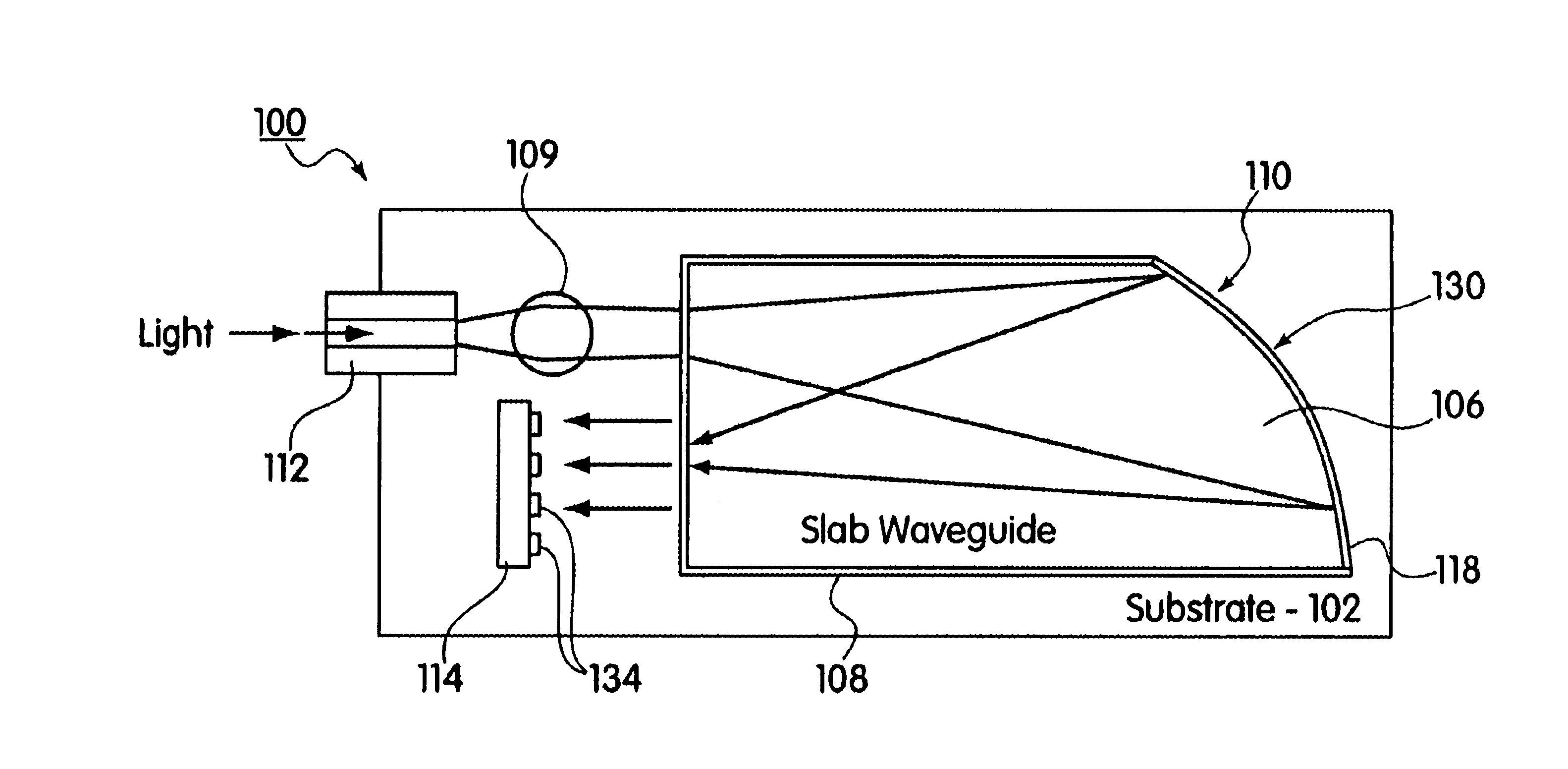
Referring to FIG. 9, a schematic layout of an illustrative spectrograph substrate 600 is shown in accordance with one embodiment of the present invention (see also, FIGS. 3 and 4). The layout and dimensions illustratively shown in FIG. 9 are those of an etched recess, for a preferred 10 GbE CWDM spectrograph design incorporating a slab waveguide. These d...


PUM


Abstract

A planar spectrograph for demultiplexing optical wavelength signals includes a monolithic substrate. The substrate has a diffraction grating etched therein. The diffraction grating is integrally formed in the substrate to be in operative relationship with input light to diffract and reflect the input light to a detector. A recess is formed in the substrate to accommodate a separate slab waveguide. A slab waveguide is dimensioned and configured to fit within the recess, and the waveguide guides input light to and from the diffraction grating. A silicon-on-insulator spectrographs is also described, as well as, fabrication processes for manufacturing these spectrographs.

Description

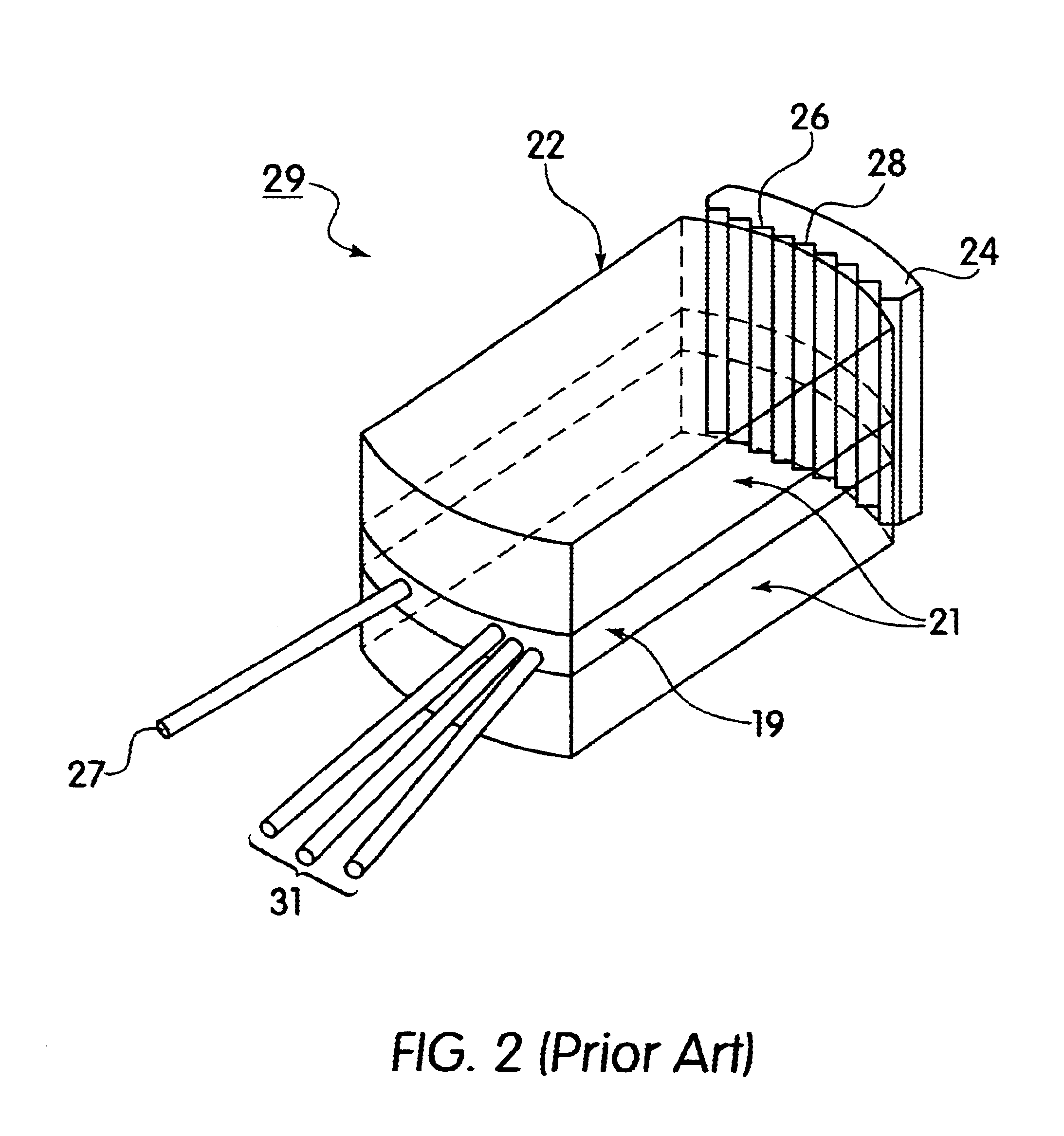
1. Field of the InventionThe present invention relates to multimode planar spectrographs and methods for their fabrication, and more particularly to planar spectrographs for demultiplexing coarse wavelength division multiplexed (CWDM) optical signals, and methods for fabrication of such spectrographs employing silicon-based processing.2. Description of the Related ArtEmerging applications of wavelength-division-multiplexing (WDM) in local-area networks require wavelength demultiplexers that are compact, low-cost, manufacturable in high volumes, and most of all compatible with multimode fiber input. Multimode operation precludes the many single-mode waveguide demultiplexers used in dense WDM systems for telecommunications purposes.A planar spectrograph demultiplexer is a two-dimensional grating spectrometer comprised of a slab waveguide which confines the light in the vertical direction and a concave reflection grating which simultaneously diffracts and images the input light, separa...

Claims


Application Information

Patent Timeline
IPC IPC(8): G01J3/28G02B6/34
CPCG02B6/12007G01J3/2803G01J3/28G02B6/4215G02B6/29326G02B6/29328G01J3/0259
Inventor COHEN, MITCHELL S.SEFLER, GEORGE A.SPEIDELL, JAMES L.
Owner IBM CORP
Learn More