Adjustable nanopore, nanotome, and nanotweezer

a nanopore and nanotome technology, applied in the direction of optical light guides, fluid speed measurement, osmosis/dialysis, etc., can solve the problems of inability to precisely predict or control the passage of an individual molecule through the pore, and the progress of nanomanipulation is slow

Inactive Publication Date: 2004-03-16
AGILENT TECH INC
View PDF7 Cites 54 Cited by
  • Summary
  • Abstract
  • Description
  • Claims
  • Application Information

AI Technical Summary

Problems solved by technology

However, progress in nanomanipulation has been slow.
One problem with these techniques is that the passage of an individual molecule through a pore cannot be precisely predicted or controlled; it is a random, stochastic event, and when a molecule enters the pore, it zips through quickly.

Method used


Image

  • Adjustable nanopore, nanotome, and nanotweezer
  • Adjustable nanopore, nanotome, and nanotweezer
  • Adjustable nanopore, nanotome, and nanotweezer

Examples


embodiment 600

As one example, FIGS. 6a-6b illustrate an alternative embodiment 600 of the invention. Through-hole 602 exists in membrane 604. The through-hole 602 may be formed, for example, by sculpting with an argon ion beam in a membrane 604 of silicon nitride as described in J. Li et al, "Ion-beam sculpting at nanometer length scales", Nature, Vol. 412, pp. 166-169 (Jul. 12, 2001). A similar hole 606, formed, for example, by the same techniques, exists in membrane 608, which membrane can also be made of silicon nitride. The two membranes, which can for example be supported on frames (not shown) of single-crystal silicon, are placed in contact or near contact, and hole 602 is placed to intersect an edge of hole 606 to form an arched opening 610 through which a sphere 612 of diameter 614 may pass. The crown of the arch is a point 616, the springer points of the arch are at points 618 and 620, and the base of the arch is formed by the edge portion 622 of through-hole 606.

embodiment 700

Another alternative embodiment 700 of the invention is illustrated in FIGS. 7a-7b. Hole 702 in membrane 704 is formed by means similar to those used to form hole 602. Edge 706 of body 708 is part of edge 710 which bounds a planar surface of body 708. Edge 706. intersects hole 702 to form an arched opening 712 through which a sphere 714 of diameter 716 may pass. The crown of the arch is point 718, the springer points of the arch are points 720 and 722, and the base of the arch is formed by edge 706. Body 708 is formed by means of, for example, chemical vapor deposition, photolithography, and etching on a surface of substrate 724 which is later etched to form cantilever 726. Cantilever 726 may contain sensing means (not shown), such as piezoresistive sensors to monitor the contact force between membrane 704 and body 708. Such sensing means are well known to those skilled in the art of atomic force microscopy. Cantilever 726 may contain actuation means (not shown), such as piezoelectri...
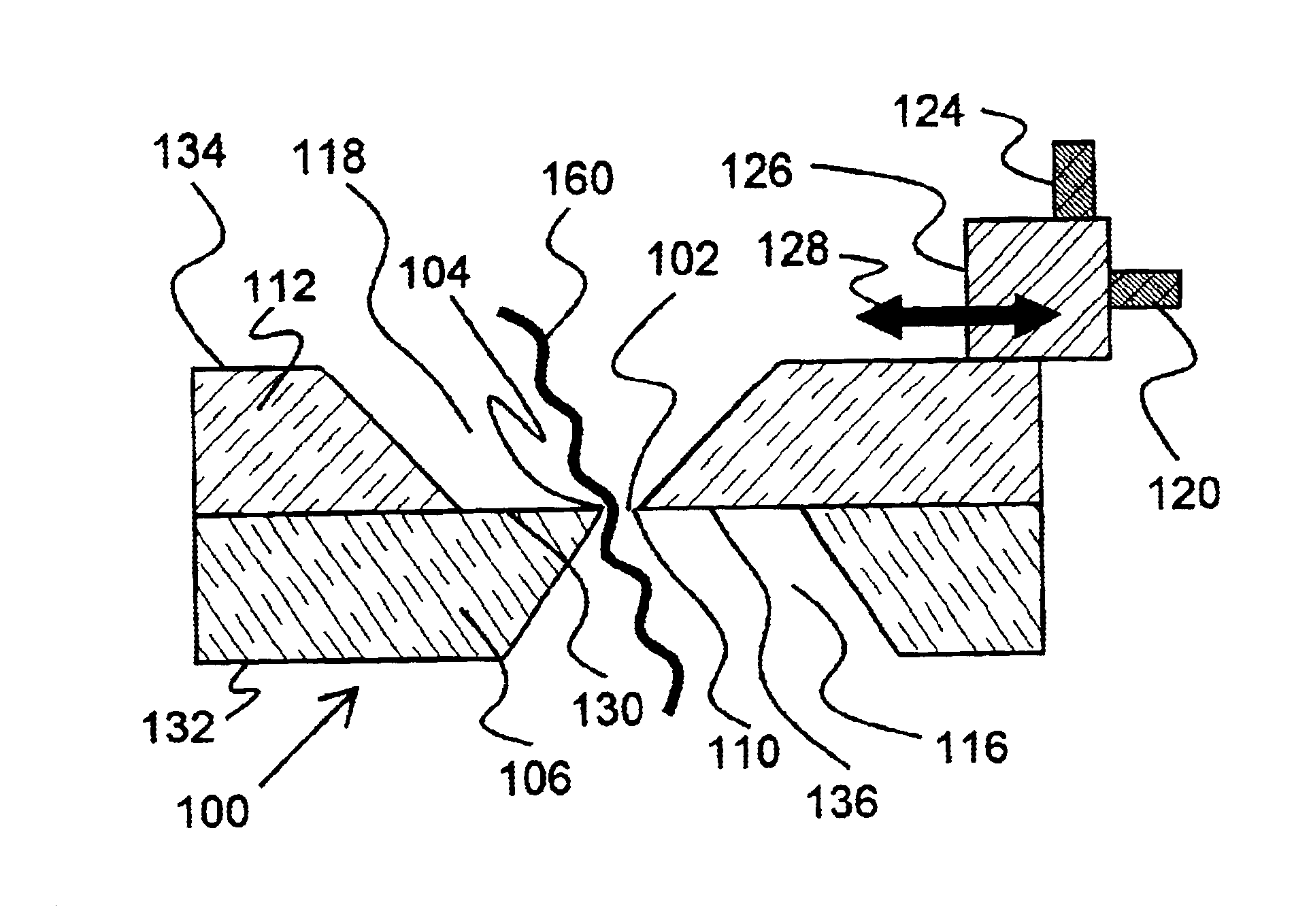
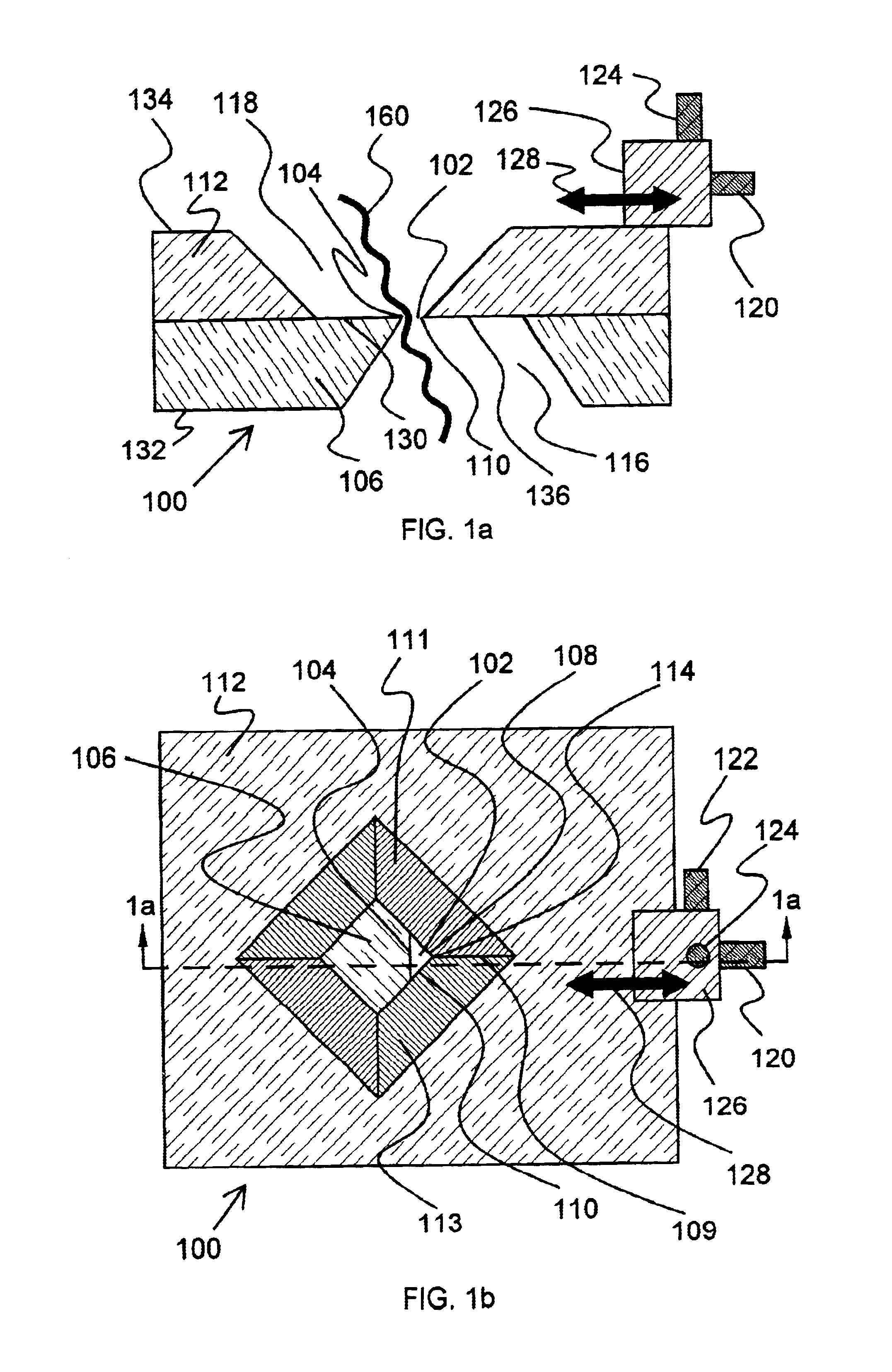
embodiment 100

Variations on the structures described above may occur to those skilled in the art without departing from the scope and spirit of the present invention. For example, other cantilever structures such as those employed in STM and AFM apparatus may be incorporated into the structure of the present invention, and other flexible structures comprising springs, beams, and flexures may be incorporated into the structure of the present invention. Sensing means such as piezoelectric sensors, optical sensors, and other types of sensors may be incorporated into the present invention to aid in detecting the relative positions of the structural components of the present invention, and to aid in detecting the force with which such structural components bear upon one another. Layers such as elastomeric layers and polymeric brushes may be incorporated, for example between surfaces 130 and 136 of embodiment 100, for purposes such as elastically filling in local surface roughness.

INDUSTRIAL APPLICABIL...


PUM

PropertyMeasurementUnit
distanceaaaaaaaaaa
distanceaaaaaaaaaa
distanceaaaaaaaaaa

Abstract

An adjustable nanopore is fabricated by placing the surfaces of two planar substrates in contact, wherein each substrate contains a hole having sharp corners and edges. A corner is brought into proximity with an edge to define a triangular aperture of variable area. Ionic current in a liquid solution and through the aperture is monitored as the area of the aperture is adjusted by moving one planar substrate with respect to the other along two directional axes and a rotational axis. Piezoelectric positioners can provide subnanometer repeatability in the adjustment process. The invention is useful for characterizing, cleaving, and capturing molecules, molecular complexes, and supramolecular complexes which pass through the nanopore, and provides an improvement over previous devices in which the hole size of nanopores fabricated by etching and / or redeposition is fixed after fabrication.

Description

The present invention relates generally to handling, measurement, and cleavage of objects at the molecular size scale, that is, with handling, measurement, and cleavage of objects with characteristic dimensions on the order of nanometers.The art of manipulating individual atoms, molecules, and supramolecular particles is called "nanomanipulation", and is in a very crude state in the year 2001.The art of nanomanipulation was first proposed by Richard Feynman on Dec. 29, 1959, at the annual meeting of the American Physical Society in a speech titled "There's Plenty of Room at the Bottom", in which he noted that"The principles of physics, as far as I can see, do not speak against the possibility of maneuvering things atom by atom. It is not an attempt to violate any laws; it is something, in principle, that can be done; but in practice, it has not been done because we are too big."Feynman, the winner of the 1965 Nobel Prize in physics, further noted in his 1959 speech that "The problem...

Claims


Application Information

Patent Timeline
Patent Type & Authority Patents(United States)
IPC IPC(8): B01D69/00B01D71/00B01D71/02B01D67/00B01D69/12B01D69/02B81B1/00
CPCB01D67/0058B01D67/0072B01D69/02B01D69/12B01D71/02B81B3/0059B81B5/00B81C99/002G01N33/48721B01D2325/02B81B2201/0214B81B2201/047B81B2203/0353B82Y30/00B82Y15/00
Inventor BARTH, PHILIP W.ROITMAN, DANIEL B.MYERSON, JOEL
Owner AGILENT TECH INC
Why Eureka
Try Eureka