

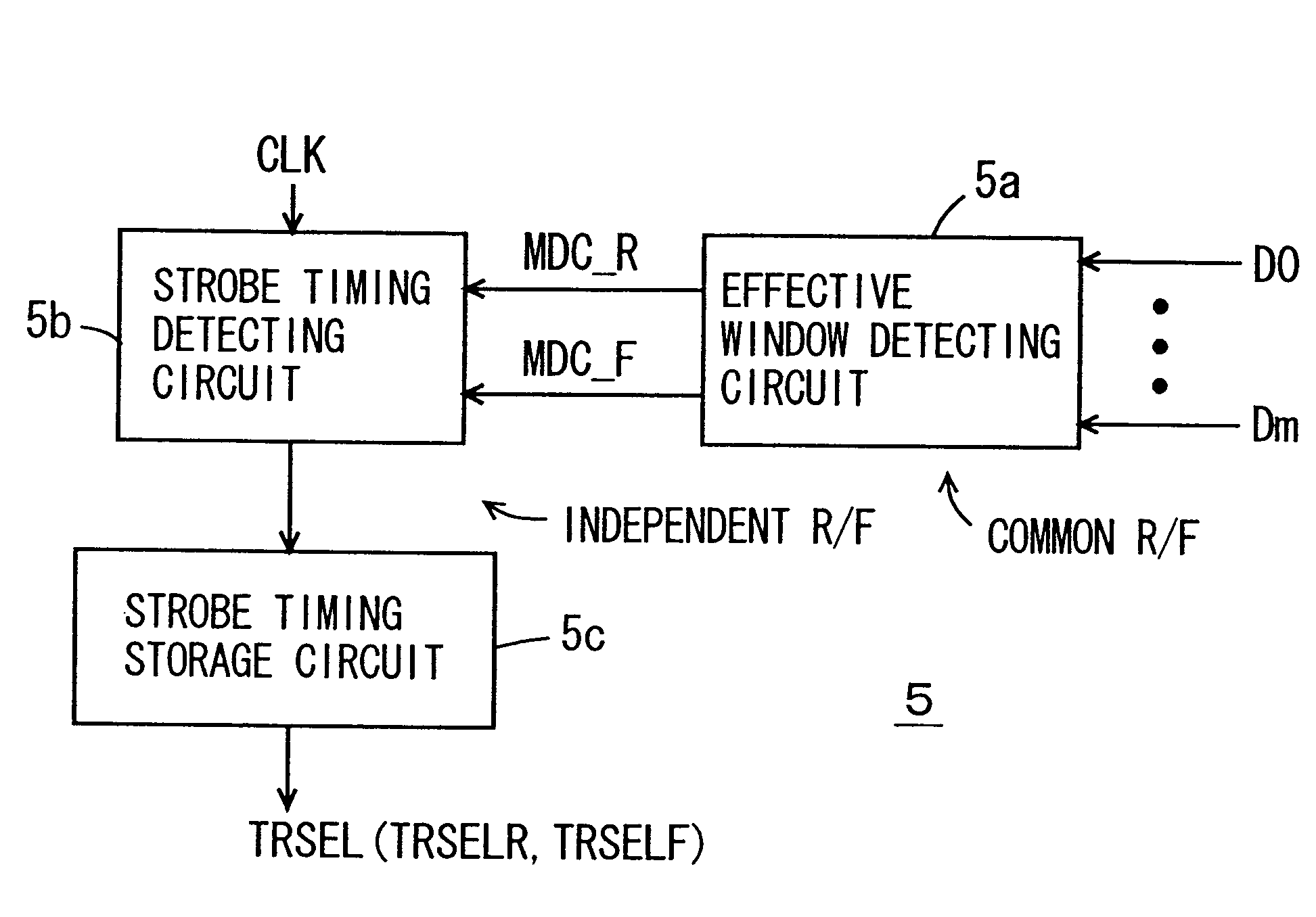
Interface circuit device for performing data sampling at optimum strobe timing by using stored data window information to determine the strobe timing
a data sampling and data window technology, applied in the field of interface circuits, can solve the problems of increasing the cost of the memory unit, unable to take in accurate data in many cases, and low design flexibility
- Summary
- Abstract
- Description
- Claims
- Application Information
AI Technical Summary
Benefits of technology
Problems solved by technology
Method used
Image

Examples
Embodiment Construction
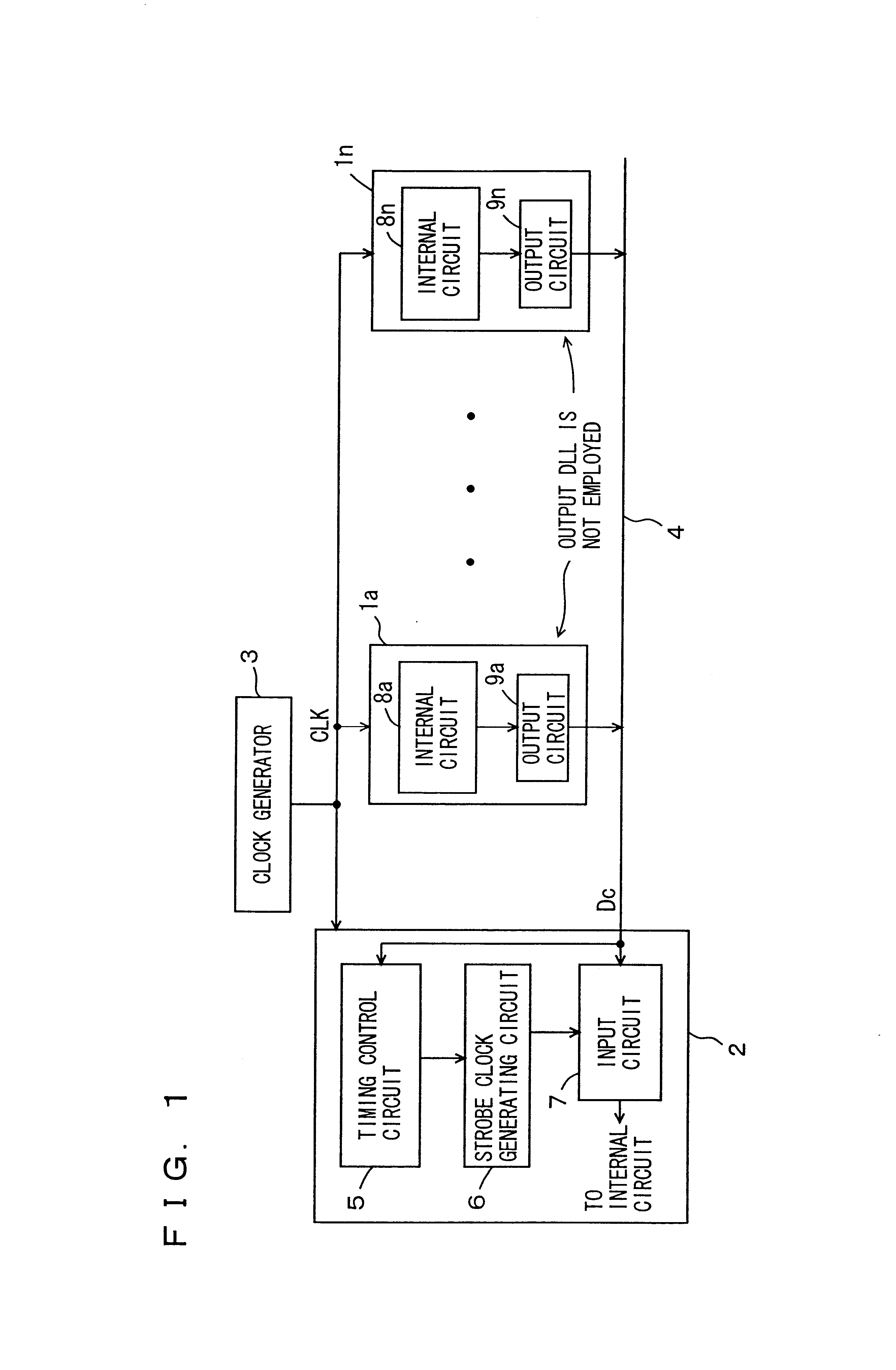
Description has been given on the memory devices that perform the data transfer at the double data rate (DDR) mode. However, the memory device employed in the present invention may be a device, which in turn transfers the data in synchronization with one of the rising and falling edges of the clock signal, or in an EDO mode. Further, the memory device may be a flash memory.
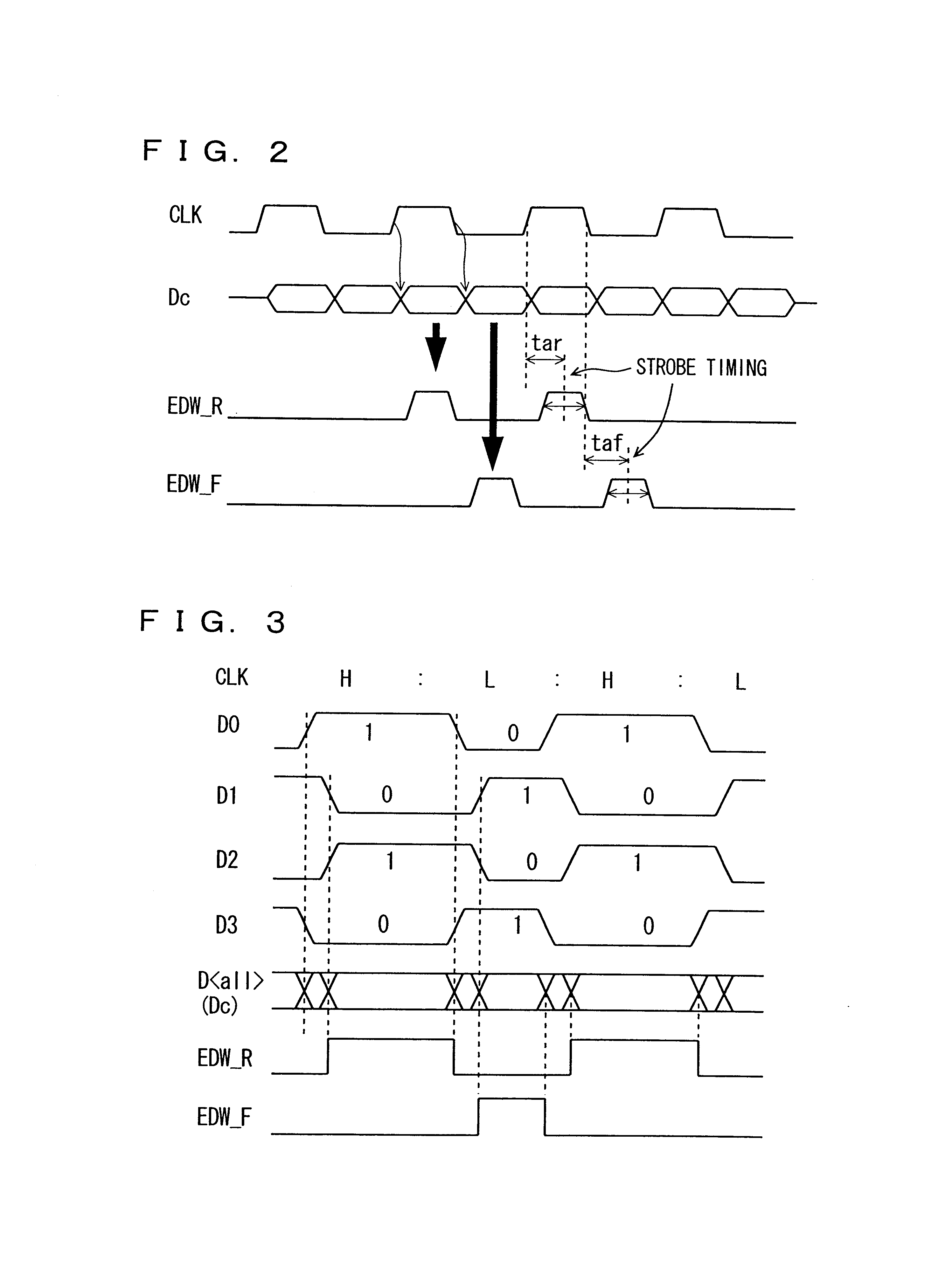
According to the present invention, as described above, the data window is detected from the data on the data line for optimizing the data strobe timing, and therefore the data transfer can be performed accurately regardless of the system structure. In the case of a memory system, a DLL for producing a data outputting clock is not required, and therefore the chip area and the power consumption can be reduced. Further, the data window width is monitored on a data receiving side, so that transfer of erroneous data can be prevented, and the reliability of the system can be ensured.
Although the present invention has b...
PUM
 Abstract
Description
Claims
Application Information