Method for designing a semiconductor integrated circuit which includes consideration of parasitic elements on critical data paths

a technology of integrated circuits and parasitic elements, applied in computer aided design, program control, instruments, etc., can solve the problems of affecting the operation speed of the circuit even more, and it takes an enormous amount of time to process a huge number of graphics patterns for a large-scale integrated circuit, so as to achieve the effect of extracting parasitic elements much more efficiently and quickly

Inactive Publication Date: 2004-05-04
SOCIONEXT INC
View PDF16 Cites 18 Cited by
  • Summary
  • Abstract
  • Description
  • Claims
  • Application Information

AI Technical Summary

Benefits of technology

According to the fifth method, at least one of the paths, of which the estimated delay exceeds a predetermined amount of time, is sorted out as a target path. Or the length of at least one pair of interconnection lines, which are included in two adjacent ones of the paths and are substantially parallel to each other, is estimated in accordance with the layout data and at least two of the paths, in which the estimated length of the parallel interconnection lines exceeds a predetermined length, are sorted out as the target paths. Then, parasitic elements are extracted from at least one of the graphics patterns, corresponding to the target paths, in accordance with the layout data. Thus, according to the present invention, there is no need to extract the parasitic elements from all the paths anymore. As a result, the parasitic elements can be extracted much more efficiently and...

Problems solved by technology

This is because the operation speed of the circuit will be affected even more seriously by those parasitic elements like wire resistance and capacitance components.
Accor...

Method used


Image

  • Method for designing a semiconductor integrated circuit which includes consideration of parasitic elements on critical data paths
  • Method for designing a semiconductor integrated circuit which includes consideration of parasitic elements on critical data paths
  • Method for designing a semiconductor integrated circuit which includes consideration of parasitic elements on critical data paths

Examples


embodiment 1

Hereinafter, a first embodiment of the present invention will be described with reference to the accompanying drawings.

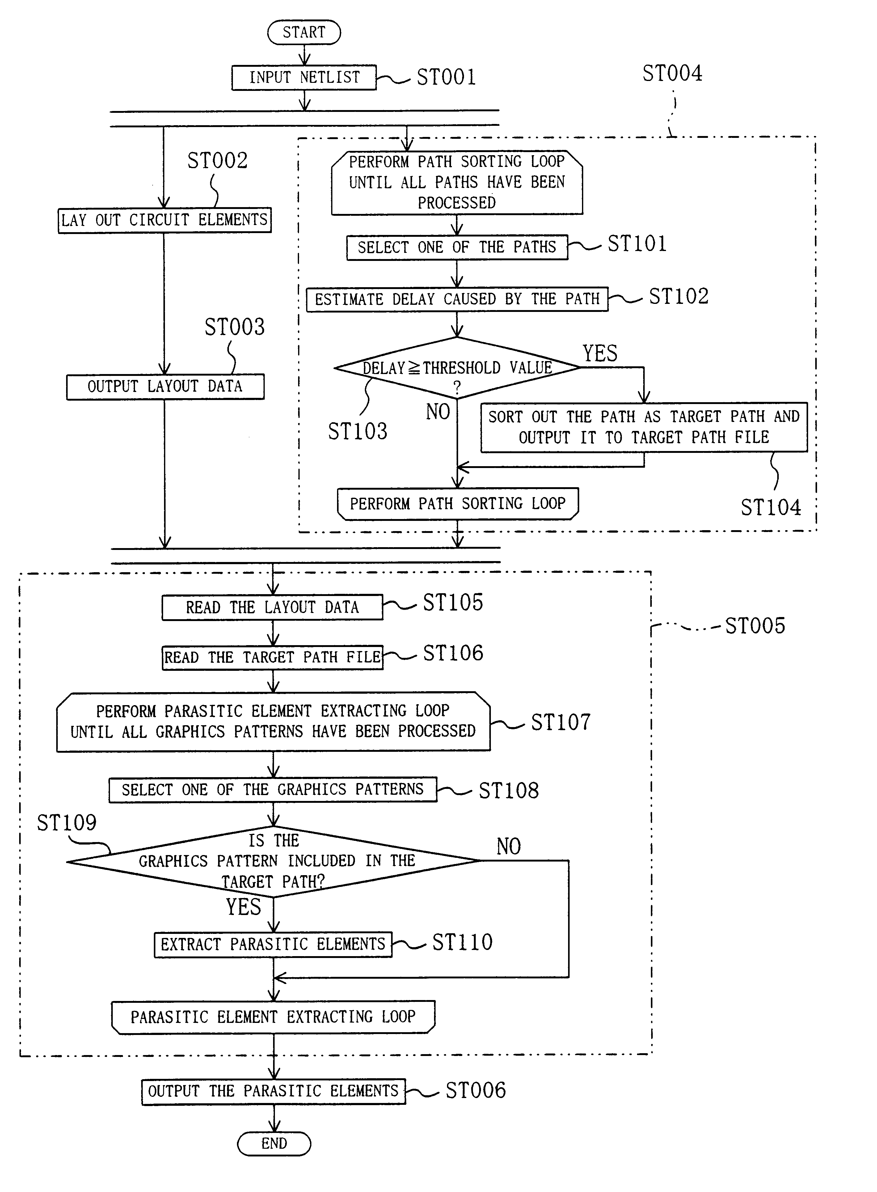
FIG. 1 illustrates the flow of a process for extracting parasitic elements in a method for designing a semiconductor integrated circuit according to the first embodiment. In the illustrated embodiment, input data such as a netlist and output data like layout data are both supposed to have to file format that can be handled by a computer-aided design tool controlled by a central processing unit (CPU).

First, in Step ST001, a netlist is read. The netlist describes topology information about interconnections among multiple circuit elements (e.g., logic devices) that will together make a semiconductor integrated circuit, on which timing analysis (or simulation) should be carried out. Generally speaking, a netlist describes only information about interconnections among the terminals of circuit elements, not information about the wire lengths of interconnection lines or ar...

embodiment 2

Next, a second embodiment of the present invention will be described with reference to the accompanying drawings.

FIG. 7 illustrates the flow of a process for extracting parasitic elements in a method for designing a semiconductor integrated circuit according to the second embodiment. In FIG. 7, the same process steps as those illustrated in FIG. 1 are identified by the same reference numerals.

First, in Step ST001, a netlist is read. The netlist describes topology information about interconnections among multiple circuit elements that will together make a semiconductor integrated circuit, on which timing simulation should be carried out.

Next, in Step ST002, the respective circuit elements are physically placed in their layout areas and interconnected together in accordance with the interconnection information described in the netlist read, thereby generating layout data.

Then, in Step ST010, graphics patterns, corresponding to interconnection lines, are extracted from the layout data ...

embodiment 3

Next, a third embodiment of the present invention will be described with reference to the accompanying drawings.

FIG. 11 illustrates the flow of a process for extracting parasitic elements in a method for designing a semiconductor integrated circuit according to the third embodiment. In FIG. 11, the same process steps as those illustrated in FIG. 7 are identified by the same reference numerals.

First, in Step ST001, a netlist is read. The netlist describes topology information about interconnections among multiple circuit elements that will together make a semiconductor integrated circuit, on which timing simulation should be carried out.

Next, in Step ST002, the respective circuit elements are physically placed in their layout areas and interconnected together in accordance with the interconnection information described in the netlist read, thereby generating layout data.

Then, in Step ST012, at least one pair of mutually adjacent graphics patterns are sorted out from the graphics patt...


PUM


Abstract

In a layout data forming step and a layout outputting step after a netlist is read, layout data is formed based on the netlist. In a path sorting step in parallel with these steps, a delay for each path is calculated based on the netlist to compare with a predetermined delay. Only a path having a delay exceeding the predetermined delay is output as a target path to an extraction path file. Then in a parasitic element extracting step, parasitic elements are extracted only from a graphic pattern included in the target path in the layout data while referencing the extraction path file.

Description

BACKGROUND OF THE INVENTIONThe present invention relates to a method for designing a semiconductor integrated circuit with parasitic elements extracted from layout data to analyze the operation timing of circuit elements.As the design rule for a semiconductor integrated circuit fabrication process has been reduced year after year, it has become increasingly important to analyze the operation timing of circuit elements, included in the circuit being designed, even more accurately by extracting various parasitic elements therefrom. This is because the operation speed of the circuit will be affected even more seriously by those parasitic elements like wire resistance and capacitance components. Thus, in the timing simulation, it should be estimated as accurately as possible how much delay will be caused by the parasitic elements that are unavoidably added to every interconnection line.In a known semiconductor integrated circuit design process, the parasitic elements should be extracted...

Claims


Application Information

Patent Timeline
IPC IPC(8): G06F17/50G06F9/45H01L21/70H01L21/82
CPCG06F17/5031G06F17/5036G06F30/3312G06F30/367
Inventor AKASHI, TERUO
Owner SOCIONEXT INC
Why Eureka
Try Eureka