Electronic assembly having high interconnection density

a technology of interconnection density and electronic components, applied in the association of printed circuit non-printed electric components, semiconductor/solid-state device details, instruments, etc., can solve problems such as insufficient heat removal systems, and affecting the performance of electronic components

Inactive Publication Date: 2004-06-22
ALCATEL LUCENT SAS
View PDF14 Cites 3 Cited by
  • Summary
  • Abstract
  • Description
  • Claims
  • Application Information

AI Technical Summary

Benefits of technology

An object of the invention is to remedy the above-mentioned problem by proposing an electronic assembly provided with a cooling device and also proposing interconnection means for the electronic module, the interconnection means being distinct from the cooling device. The advantage of the invention is to make use of the three-dimensional structure of the electronic module to separate the interconnection function and the heat removal function, thereby enabling each of these functions to be optimized independently of the other.
In addition, the entire second face of the module can be used for providing interconnection functions, and none of its area needs to be set aside for removing heat. Consequently, the invention makes it possible to propose a module that offers a greater density of interconnections.
In the state of the art, modules are known that are provided with optical interconnection means. Optical interconnection means present the advantage of being insensitive to the electromagnetic fields created in environments of the kind that surround modules of the invention. In addition, optical interconnections present the advantage of making it possible to achieve a greater density of interconnections than when using electronic interconnections.
Another object of the invention is to remedy the problems mentioned by proposing a module having optical interconnection means that make it possible to avoid the presence of specific transfer means to guarantee the alignment accuracy that is required for such optical interconnections. The optical interconnection means of the invention no longer require the presence of a connector unit. The invention provides for an optical fiber, e.g. included in a printed circuit, to be put into register with an optical contact of the module merely by mounting the printed circuit with precision on a face of the module that has the optical contact. The precision mounting implemented is compact since the contact points between the printed circuit and the face are limited to micropoints that are disposed very accurately respectively on the face of the module and on the printed circuit. Thereafter, these micropoints are interconnected by capillarity during a step of melting the micropoints when they are at a very small distance apart from one another.
This method of bringing points into register thus enable the density of the optical connectors presented by such an electronic module to be increased because the space required for the specific transfer means of the optical connectors is now available to present additional optical contacts.

Problems solved by technology

The state of the art assembly raises a problem since it firstly prevents the module from providing interconnections at high density.
Secondly, the heat removal system that is provided is not sufficient since it is made in the printed circuit card, even through firstly the amount of heat to be removed is large and secondly the removal system cannot be too large in size given the miniaturization conditions imposed on such integrated modules and printed circuit cards.
Furthermore, the card cannot receive a miniature heat removal system of higher performance since it is constituted by a substrate made of a material that has poor heat conduction characteristics.

Method used


Image

  • Electronic assembly having high interconnection density
  • Electronic assembly having high interconnection density
  • Electronic assembly having high interconnection density

Examples


first embodiment

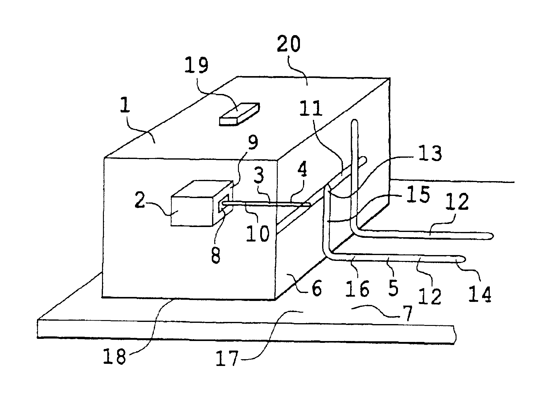
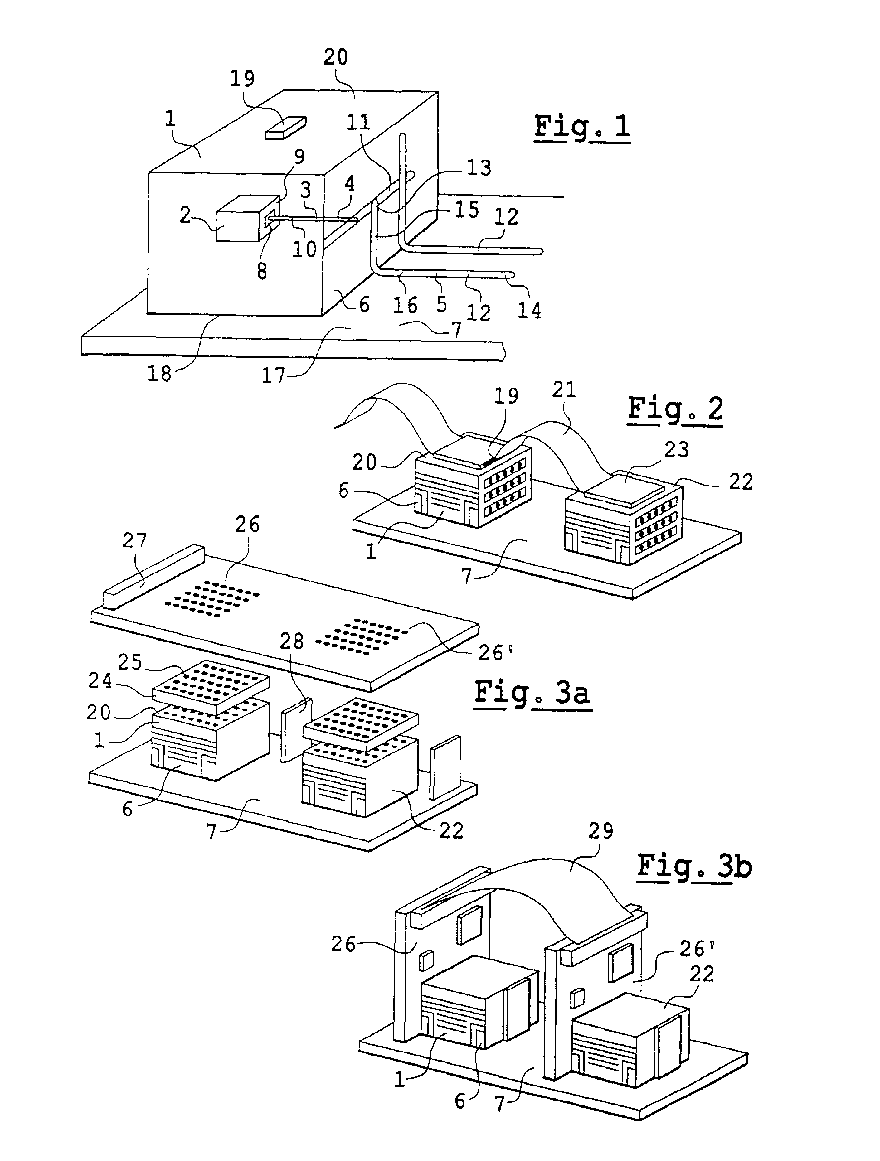
In FIG. 1, the interconnection means is a connector 19 mounted on a face 20 such that the face 20 is different from the face 18. In a first embodiment, the connector 19 is connected to a flexible printed circuit 21 to connect the module 1 to a second connector 23 on a second electronic module 22.

The second module 22 can be made in identical manner to the first electronic module 1, in which case it is likewise mounted on the top surface 17 of the soleplate 7. Under such circumstances, the second electronic module 22 also has an electronic assembly with heat removal such as 3.

In a variant, the second module 22 can be mounted on a substrate that is equivalent to that of the soleplate 7, for example so that the top faces of the modules 1 and 22 lie in a common plane.

second embodiment

In a second embodiment, as shown in FIG. 3a, the interconnection means is a contact matrix 24 comprising spring contacts 25, the contact matrix 24 being placed between a face such as the face 20 of the module 1 and a printed circuit card 26. The printed circuit card 26 can also be connected to the second module 22 as shown in FIG. 3a, for example.

third embodiment

In a third embodiment, as shown in FIG. 3b, the interconnection means is a matrix of contacts having spring contacts as shown in FIG. 3a, but also including second connection means. The second connection means comprise, for example, a printed circuit card 26' mounted on the module 22, and an intermediate flexible printed circuit 29 for connecting the printed circuit card 26 to the second printed circuit card 26'.

These printed circuit cards 26 and 26' can also have other connectors 27 for making connections with other elements. The card 26 is held to the module 1 in part by mounting the card 26 on a stiffener 28. For example, the card 26 can be screwed to the stiffener 28.

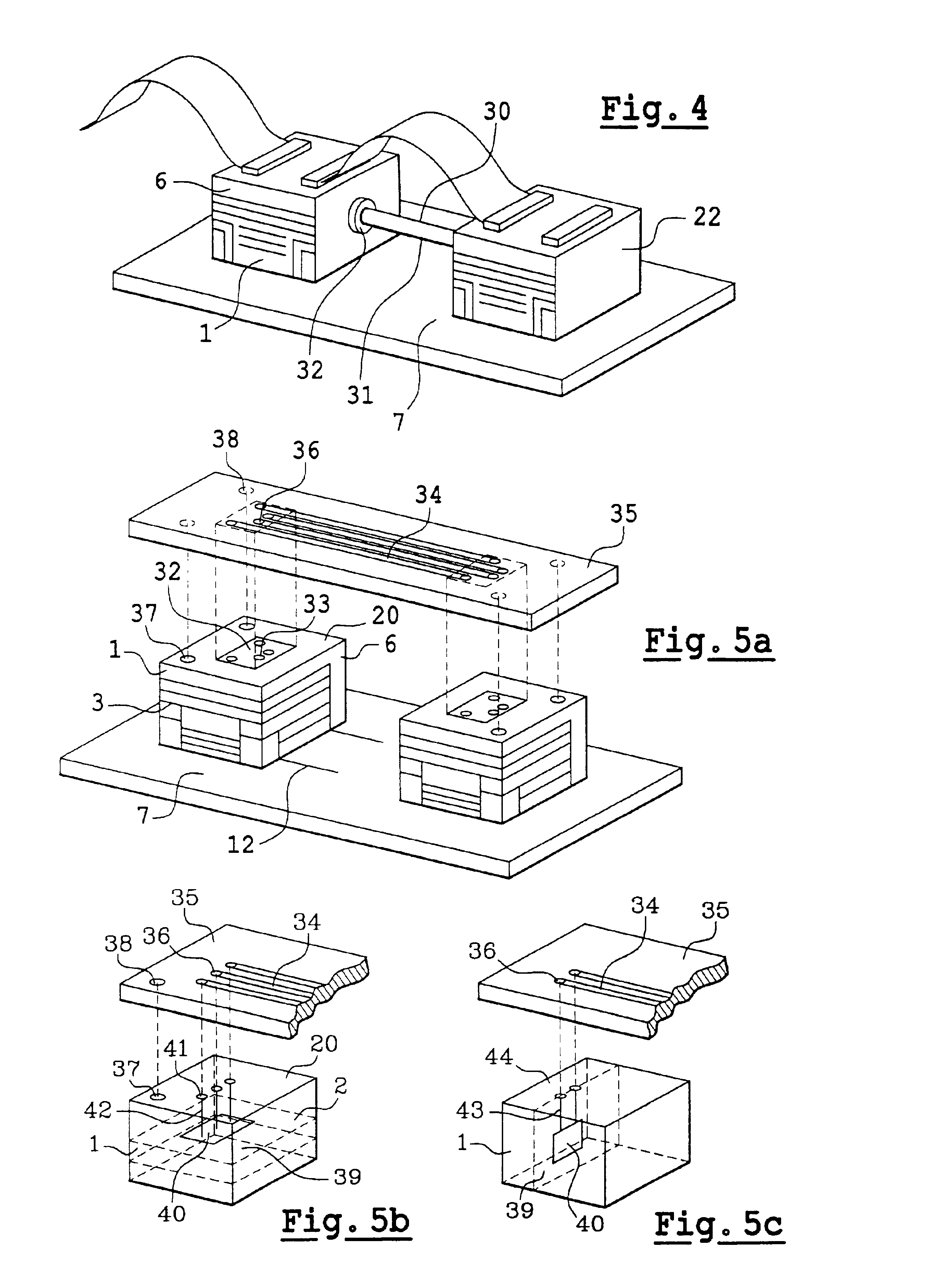
In the fourth embodiment as shown in FIG. 4, the interconnection means can be optical interconnection 30. In this fourth embodiment, the optical interconnection 30 comprises an optical fiber 31 and a first optical connector 32. The first optical connector 32 is mounted on the module 1. The optical fiber 31 can also ...


PUM


Abstract

An electronic assembly comprising an electronic module provided with optical interconnection and heat removal means, the heat removal means comprising a soleplate dedicated to removing heat on which the module is mounted. The interconnection means is independent of the soleplate and preferably comprises a printed circuit and an optical fiber included in the printed circuit. The optical fiber has an end put accurately in register with an optical contact of the module by a BGA type mounting of the printed circuit on the module. A BGA type mounting consists in placing with precision firstly balls on the module and secondly areas on the circuit, and then in bringing the balls and areas face to face so that the balls center themselves automatically with the areas by capillarity.

Description

The present invention relates to an electronic assembly having high-density interconnections. A particular application of the invention lies in the field of integrated electronic modules, i.e. modules comprising a plurality of specialized integrated circuits known as application specific integrated circuits (ASICs). These ASICs perform numerous complex functions, and for them to operate it is necessary for a large number of inlet and outlet ports on the module to be served. The field of the invention is particularly that of integrated modules of three-dimensional structure, and in a preferred example, in the form of a cube.In the state of the art, cube-shaped integrated electronic modules are known that are connected via one of their faces to a printed circuit card. The electronic module is mounted by soldering tabs on the module to transfer contacts on the card. In order to dissipate the heat given off by such a module in operation, a heat removal system is known including a heat d...

Claims


Application Information

Patent Timeline
Patent Type & Authority Patents(United States)
IPC IPC(8): H05K7/20H01R12/24H01L23/36H01L23/427H01R13/46H05K1/14H05K1/18
CPCG02B6/43H01L23/427G02B6/4214H01L2924/0002H01L2924/00
Inventor VENDIER, OLIVIERHUAN, MARCPAINEAU, SYLVAIN
Owner ALCATEL LUCENT SAS
Why Eureka
Try Eureka