Method of preparing a semiconductor having controlled crystal orientation

a technology of controlled crystal orientation and semiconductor, which is applied in the direction of semiconductor devices, electrical devices, transistors, etc., can solve the problems of reducing the reliability and electrical stability of a device using such a semiconductor, adversely affecting the properties of the device, and introducing nickel that is not sufficiently useful

Inactive Publication Date: 2004-06-29
SEMICON ENERGY LAB CO LTD
View PDF45 Cites 141 Cited by
  • Summary
  • Abstract
  • Description
  • Claims
  • Application Information

AI Technical Summary

Problems solved by technology

Nevertheless, the presence of a large amount of an element such as mentioned above in a semiconductor is not preferred because it will reduce the reliability and electrical stability of a device using such a semiconductor.
Regarding this amount, it has been found that if the nickel concentration of the active layer is not 1.times.10.sup.19 atoms / cm.sup.3 or lower then an adverse effect on the properties of the device will result.
That is, even if a large amount of nickel is introduced, it is thought that some nickel is present which is not sufficiently useful.
As a method of introducing the trace amount of nickel into only the region near the surface of the amorphous silicon film, i.e. a method for trace addition of the crystallization-promoting catalytic element into only the region near the surface of the amorphous silicon film, there may be mentioned the vapor deposition process; however, the vapor deposition process is disadvantaged by poor controllability and difficulty in strictly controlling the amount of the catalytic element introduced.
Furthermore, since the amount of the catalytic element introduced must be as small as possible there often results the problem of unsatisfactory crystallization, and thus it is important to appropriately adjust the amount of the catalytic element.
This indicates that crystallization becomes more difficult as it progresses.
However, the crystalline axes are not completely uniform as a result of limitations on the film thickness, stress, etc.
Also, an actual problem is that it is difficult to completely match the direction of crystal growth with the direction of flow of the carrier, and the crystals also fail to grow over the entire surface in a uniform direction.
However, the maximum degree to which the particle size may be increased is unconditionally determined by the dose of the above mentioned catalytic element.

Method used


Image

  • Method of preparing a semiconductor having controlled crystal orientation
  • Method of preparing a semiconductor having controlled crystal orientation
  • Method of preparing a semiconductor having controlled crystal orientation

Examples


example 1

This example illustrates the preparation of a silicon film with a high (111) orientation which involves selective provision of a 1200 .ANG. silicon oxide film which is used as a mask for selective introduction of nickel and lateral growth.

The preparation process in this example is outlined in FIG. 3. First, on an amorphous silicon film (a 500 .ANG. film prepared by plasma CVD) placed on a glass substrate (Corning 7059, 10 cm square) there is formed a silicon oxide film 21 which functions as a mask (silicon dioxide cover) to a thickness of 1000 .ANG. or more, 1200 .ANG. in this example. The inventors have experimentally confirmed that a thickness of the silicon dioxide film 21 exceeding 500 .ANG. does not cause any particular trouble, and it is believed that thinner films may be accepted as long as they have fine quality.

The silicon oxide film 21 is then patterned as desired by a conventional photolithographical patterning process. Thereafter irradiation with ultraviolet ray is condu...

example 2

This Example is for a case where entirely the same process as in Example 1 was used, varying only the thickness of the amorphous silicon film to two levels, 400 .ANG. and 800 .ANG..

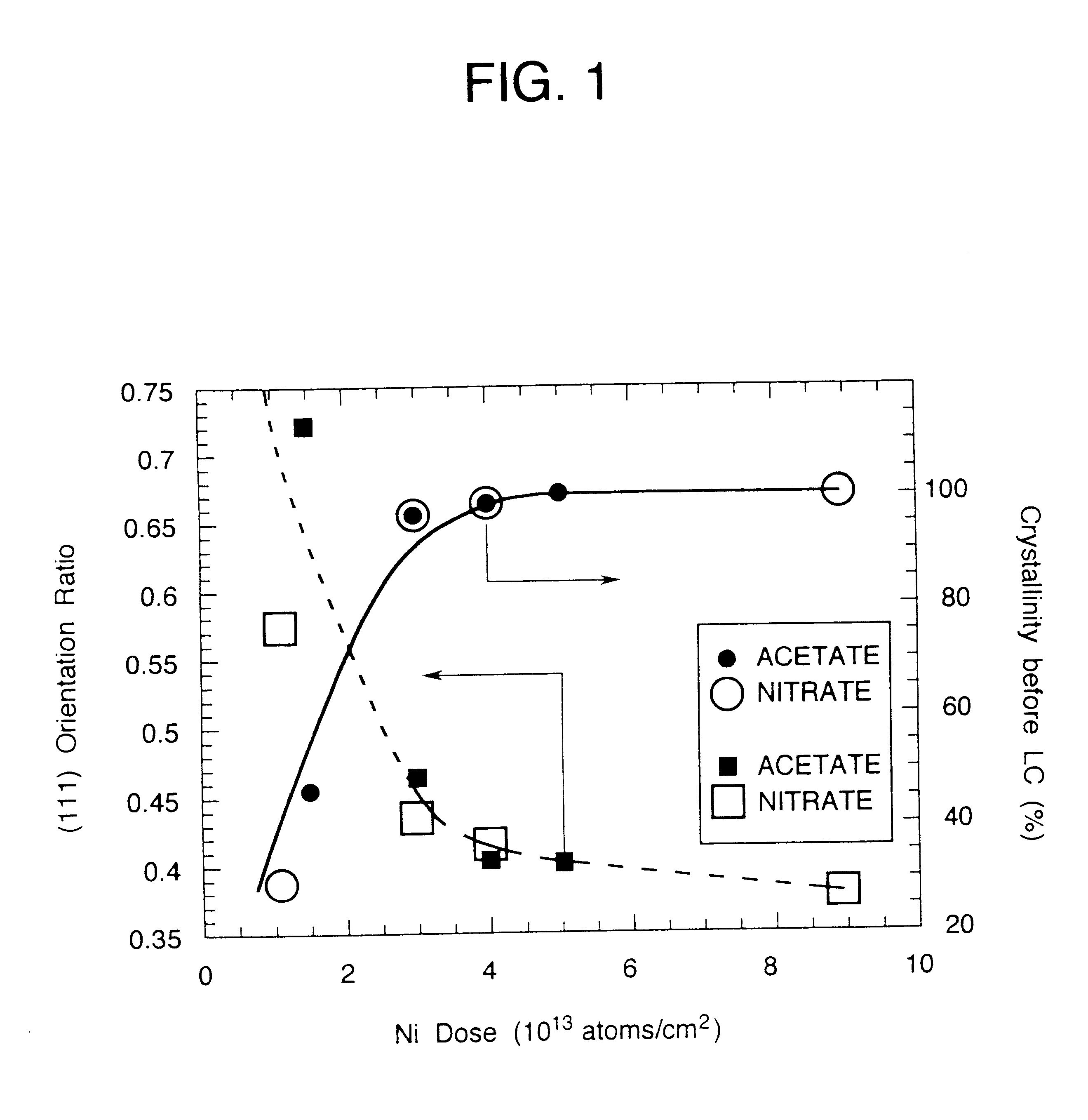
The results revealed that the (111) orientation ratio obtained with X-ray diffraction for the 400 .ANG. specimen was about 1.0, showing it to be an almost completely (111)-oriented film, while that of the 800 .ANG. specimen was 0.720, or somewhat less (111) orientation as compared with the 500 .ANG. sample.

example 3

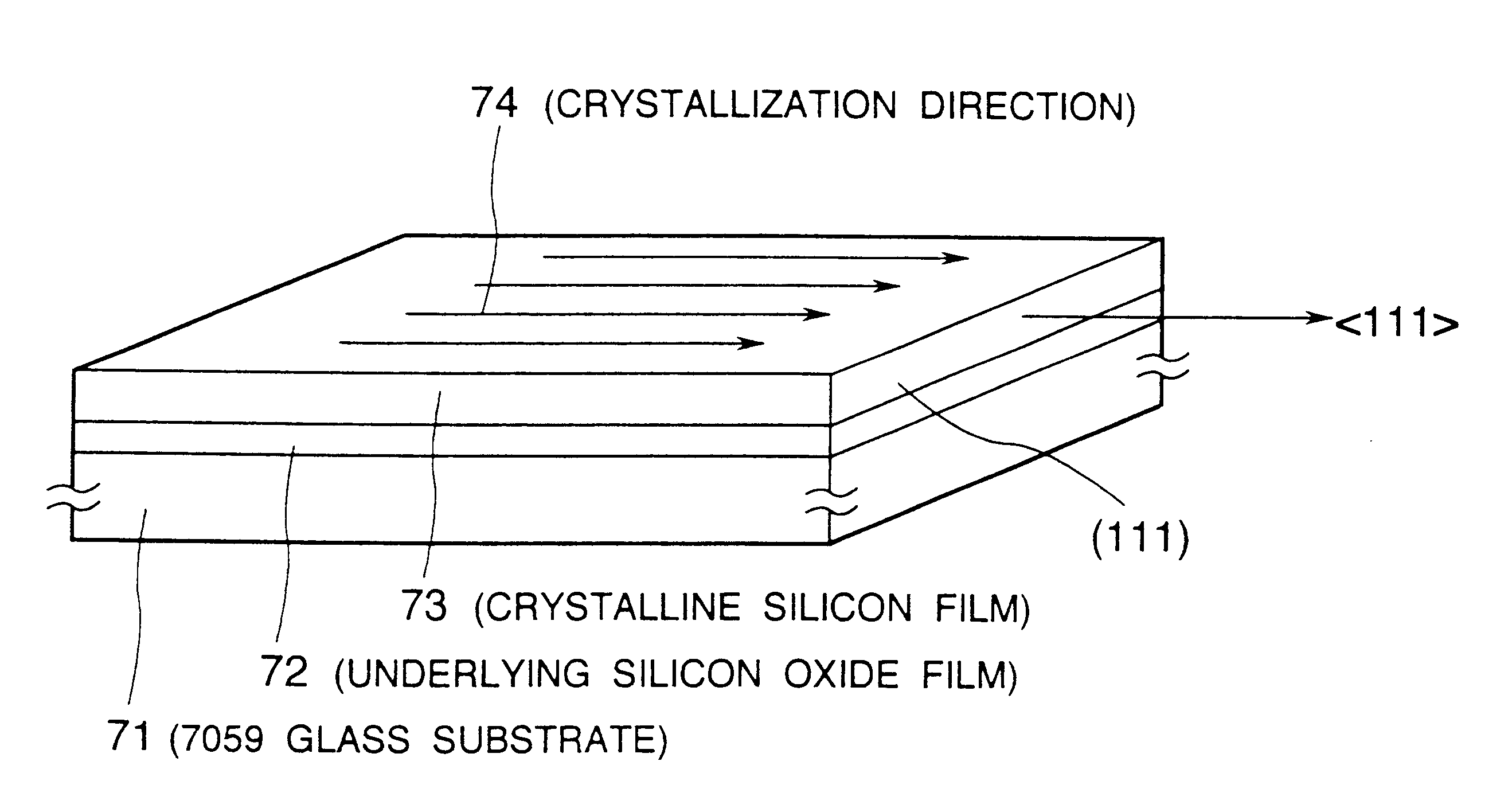
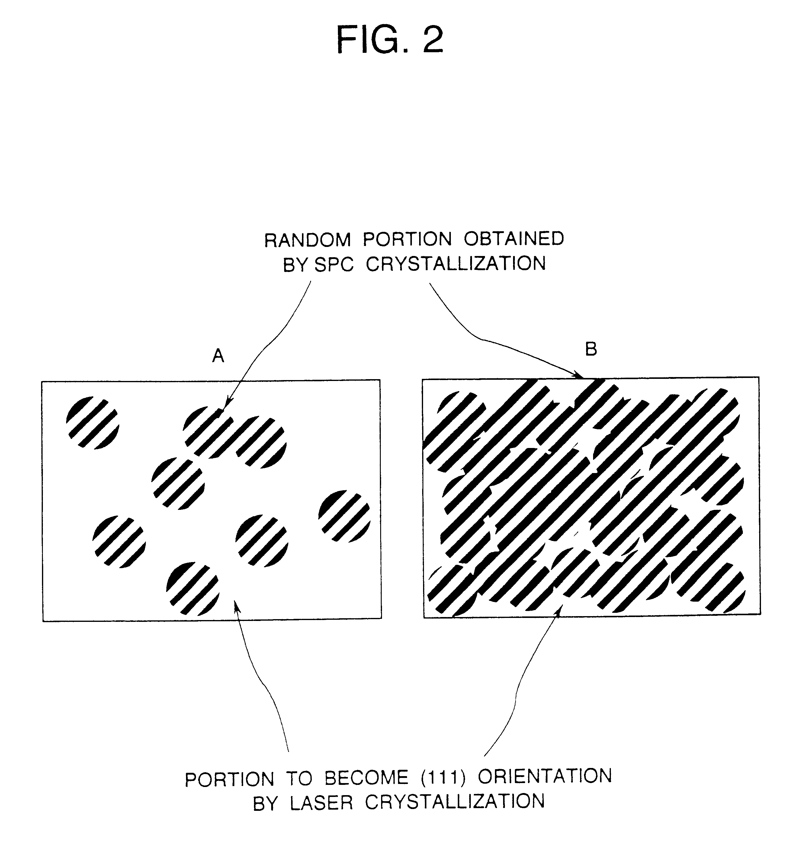
This example is for a case where a crystallization-facilitating catalytic element is contained in an aqueous solution which is then applied on an amorphous film, which is then subjected to heat for crystallization followed by irradiation with laser light for further improvement of the crystallinity. This case corresponds to the vertical growth in the previous description, and may provide a film with a relatively random orientation.

The process as far as the introduction of a catalytic element (in this case, nickel was used) will be explained with reference to FIG. 5. In this example, Corning 7059 glass is employed as the substrate 11. Its size is 100 mm.times.100 mm.

First, the amorphous silicon film 12 is formed to 100 to 1500 .ANG. by plasma CVD or LPCVD. In this particular case, the amorphous silicon film 12 is formed to a thickness of 500 .ANG. by plasma CVD (FIG. 5(A)).

Then, to remove the dirt and spontaneous oxide film, treatment with hydrofluoric acid is carried out, after whic...


PUM

PropertyMeasurementUnit
temperaturesaaaaaaaaaa
temperatureaaaaaaaaaa

Abstract

A semiconductor device is disclosed. The semiconductor device has a crystalline silicon film as an active layer region. The crystalline silicon film has needle-like or columnar crystals oriented parallel to the substrate and having a crystal growth direction of (111) axis. A method for preparing the semiconductor device comprises steps of adding a catalytic element to an amorphous silicon film; and heating the amorphous silicon film containing the catalytic element at a low temperature to crystallize the silicon film.

Description

1. Field of the InventionThe present invention relates to a semiconductor device which has a TFT (thin-film transistor) built onto an insulating substrate made of glass or the like, and to a method for its preparation.2. Description of the Prior ArtThin-film transistors (hereunder, TFTs) are known which employ thin-film semiconductors. These TFTs are constructed by forming a thin-film semiconductor on a substrate and using the thin-film semiconductor. These TFTs are used in various integrated circuits, but particular attention is being given to their use in electrooptical devices, especially as switching elements constructed for the respective picture elements of active matrix-type liquid crystal displays and driving elements formed in peripheral circuit sections.The TFTs used in these devices generally employ thin-film silicon semiconductors. Thin-film silicon semiconductors are largely classified into two types: amorphous silicon semiconductors (a--Si) and silicon semiconductors w...

Claims


Application Information

Patent Timeline
Patent Type & Authority Patents(United States)
IPC IPC(8): H01L21/02H01L21/20H01L29/66H01L29/786
CPCH01L21/2026H01L29/78675H01L21/02686H01L21/02422H01L21/02488H01L21/02532H01L21/02609H01L21/02672H01L21/02675
Inventor ZHANG, HONGYONGTAKAYAMA, TORUTAKEMURA, YASUHIKOMIYANAGA, AKIHARUOHTANI, HISASHITAKEYAMA, JUNICHI
Owner SEMICON ENERGY LAB CO LTD
Why Eureka
Try Eureka