

Gas pulsing for etch profile control
a technology of etching and gas pulsing, which is applied in the direction of electrical discharge tubes, decorative arts, electrical apparatus, etc., can solve the problems of increased difficulty in controlling the high selectivity etching process that uses these so-called "polymer gases" and the increase of the difficulty of controlling the so-called "polymer gas" process, and achieves the effect of tapered profile or etch stop
- Summary
- Abstract
- Description
- Claims
- Application Information
AI Technical Summary
Benefits of technology
Problems solved by technology
Method used
Image

Examples
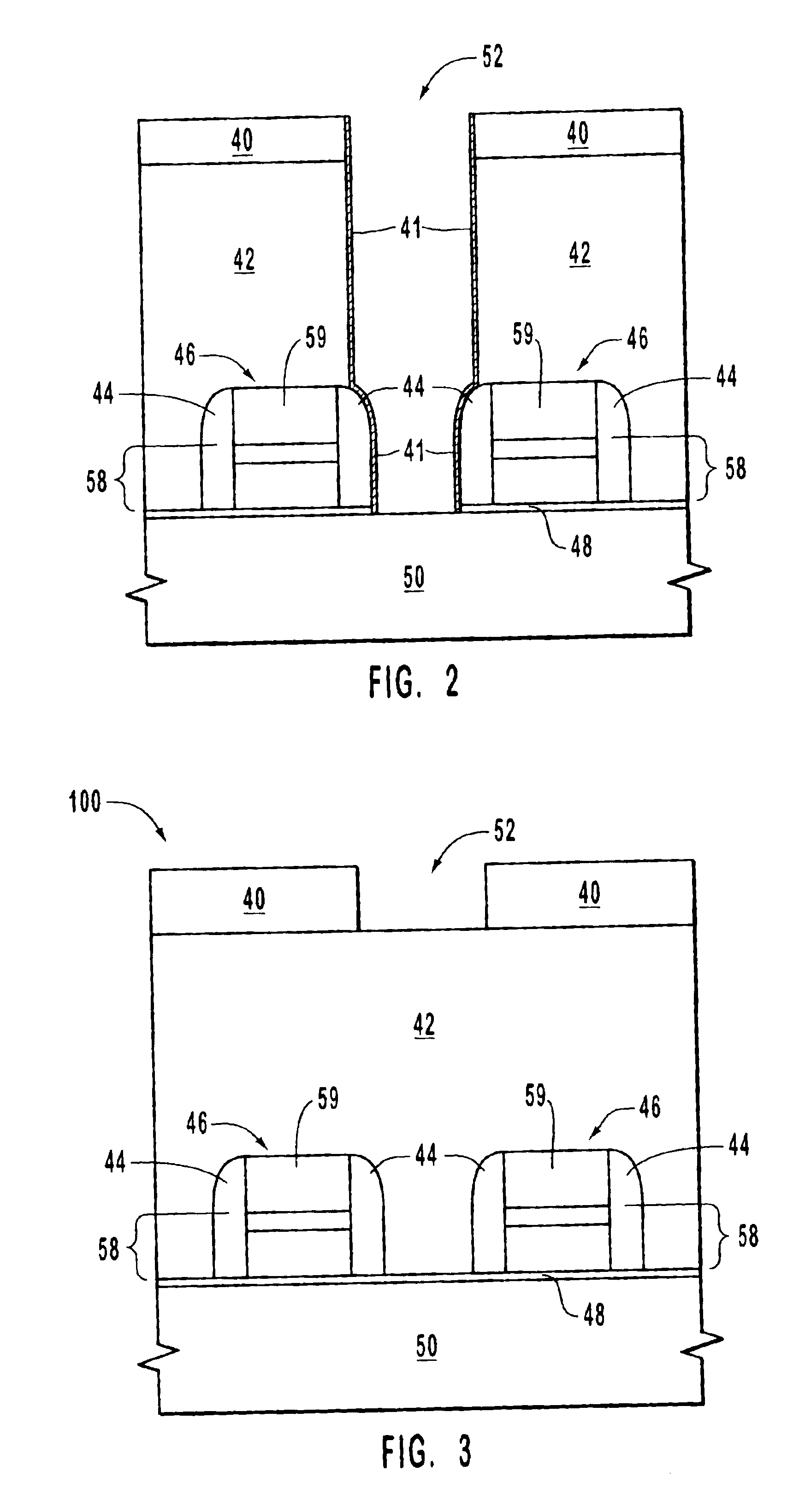
example 2
In this example, the series of steps 1 that are referred to alternatively as "1A" and "1B" run for a total of 100 s, with a duration of 10 s each. CHF.sub.3 is pulsed in steps labelled "1A" and "1B", but CH.sub.2 F.sub.2 is not pulsed. Only CHF.sub.3 is flowed in step 2 under non-pulsing conditions. The gas flow rate conditions in this example are depicted graphically in FIG. 16 for steps 1 and 2, where the solid line displays the oscillating high and low flow regimes for CHF.sub.3 in step 1. The conditions for this example are given numerically as follows:
Step 1A: 1000 w Source / 800 w Bias, 15 sccm CHF.sub.3, 20 sccm CH.sub.2 F.sub.2, 20 mTorr, 10 sec.
Step 1B: 1000 w Source / 800 w Bias, 25 sccm CHF.sub.3, 20 sccm CH.sub.2 F.sub.2, 20 mTorr, 10 sec.
Step 1A: 1000 w Source / 800 w Bias, 15 sccm CHF.sub.3, 20 sccm CH.sub.2 F.sub.2, 20 mTorr, 10 sec.
Step 1B: 1000 w Source / 800 w Bias, 25 sccm CHF.sub.3, 20 sccm CH.sub.2 F.sub.2, 20 mTorr, 10 sec.
Step 1A: 1000 w Source / 800 w Bias, 15 sccm CHF...
example 3
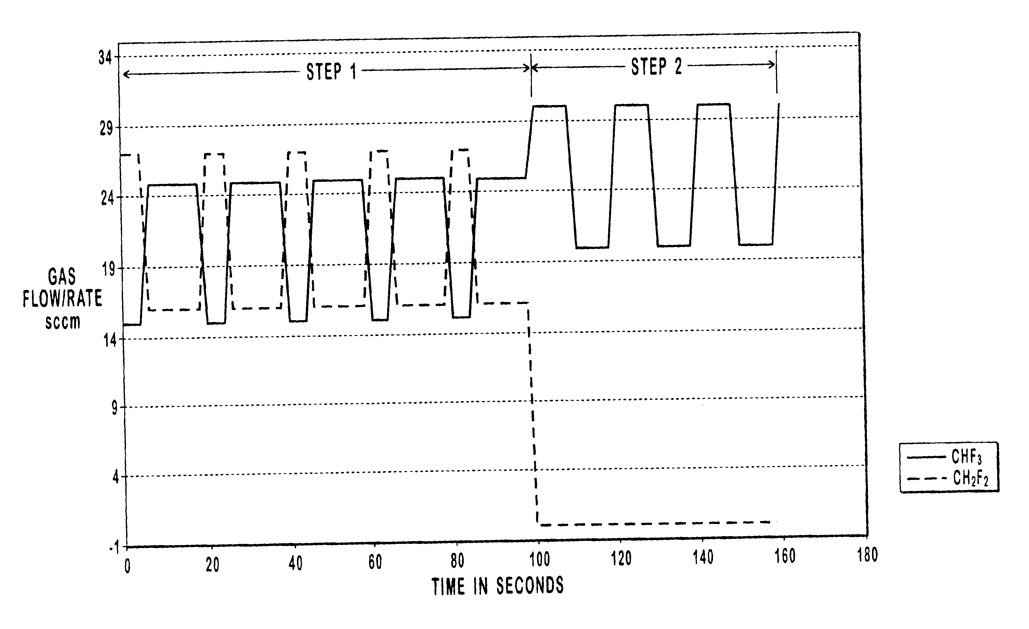
In this example, the series of steps 1 that are referred to alternatively as "1A" and "1B" are applied under pulsing conditions for both gases CHF.sub.3 and CH.sub.2 F.sub.2 as shown by the solid and dashed lines in FIG. 17 in the portion of the graph labelled "step 1". Only CHF.sub.3 is provided under pulsing conditions but no CH.sub.2 F.sub.2 is flowed in step 2, as shown by the solid and dashed lines in the portion of the graph labelled "step 2" in FIG. 17. The solid line in the same figure indicates that the high and low flow rates for CHF.sub.3 under pulsing conditions in step 1 are different from the high and low flow rates for the same gas under pulsing conditions in step 2. Note also that all gases are pulsed in both steps in this example at the same period and duty cycle. The conditions for this example are given numerically as follows:
Step 1A: 1000 w Source / 800 w Bias, 15 sccm CHF.sub.3, 27 sccm CH.sub.2 F.sub.2, 20 mTorr, 5 sec.
Step 1B: 1000 w Source / 800 w Bias, 25 sccm C...
example 4
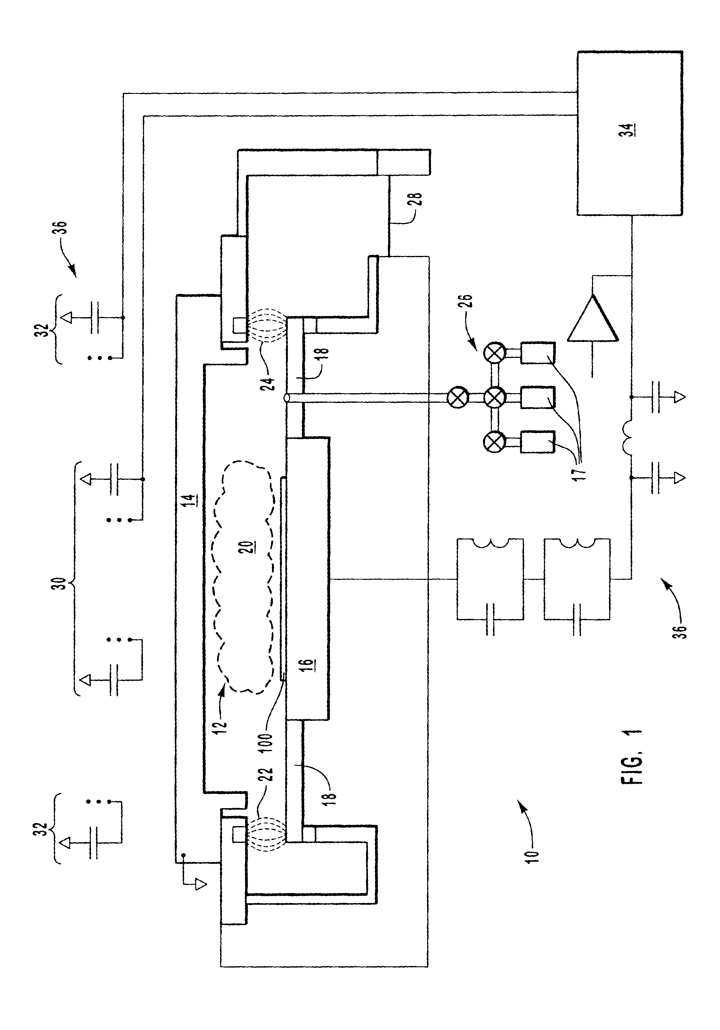
This embodiment provides an example of a flow sequence in which two gases, gas 1 and gas 2, are pulsed with different periods or duty cycles. The timing chart for this example shown in FIGS. depicts the flow rates that are controlled with external signal generators that drive the set points to the mass flow controllers.
PUM
| Property | Measurement | Unit |
|---|---|---|
| Fraction | aaaaa | aaaaa |
| Fraction | aaaaa | aaaaa |
| Fraction | aaaaa | aaaaa |
Abstract
Description
Claims
Application Information