Conductive and robust nitride buffer layers on biaxially textured substrates

Inactive Publication Date: 2004-08-31
APPL THIN FILMS INC +1
View PDF22 Cites 68 Cited by
  • Summary
  • Abstract
  • Description
  • Claims
  • Application Information

AI Technical Summary

Problems solved by technology

There are a considerable number of problems and deficiencies associated with the prior art relating t

Method used


Image

  • Conductive and robust nitride buffer layers on biaxially textured substrates
  • Conductive and robust nitride buffer layers on biaxially textured substrates
  • Conductive and robust nitride buffer layers on biaxially textured substrates

Examples


example 1

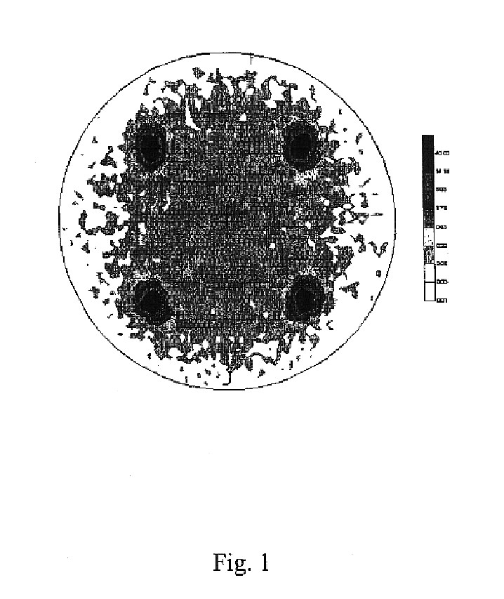
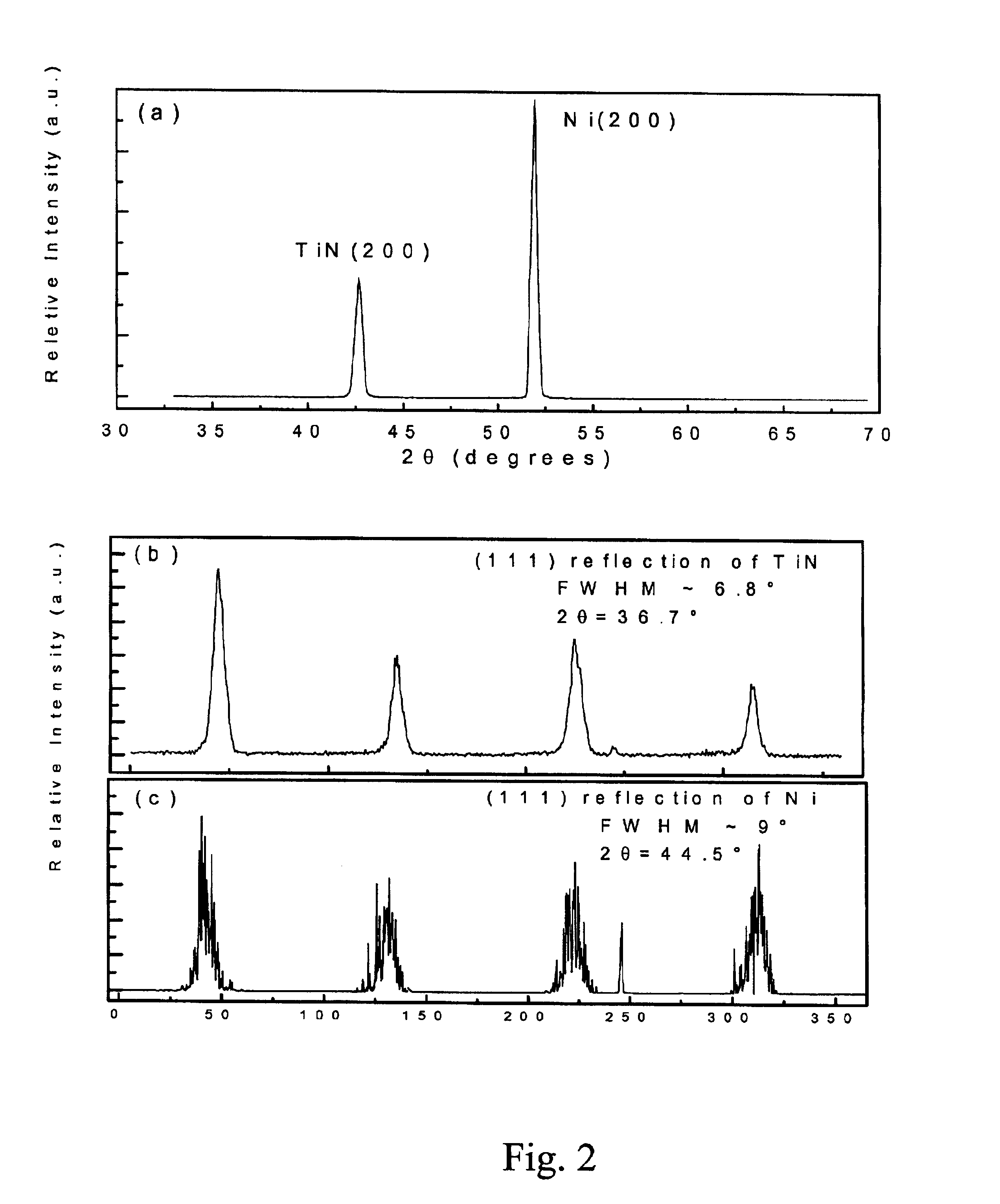
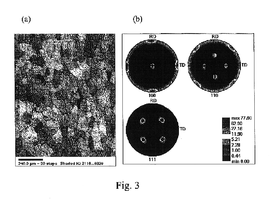
Magnetron sputtered TiN films were grown at a substrate temperature of 700.degree. C. on biaxially textured nickel substrates at a deposition rate of 1.5 Angstrom / sec. The films had a thickness of 300 nm. The films showed a remarkably low in-plane and out-of-plane alignment, FIG. 1 shows a TiN (111) pole figure. The existence of only four peaks demonstrates a single epitaxial orientation. The location of the peaks in the (111) pole figure is consistent with a cube-on-cube epitaxial relationship. The TiN (111) phi scan in FIG. 2(b) to (d) showed a full-width-half-maximum (FWHM) obtained by fitting a guassian curve to the data to be 6.6.degree.. The FWHM is slightly better than that of the underlying Ni with a FWHM of .about.7.degree.. The rocking curves or the out-of-plane texture of the TiN layer was found to be 3.9.degree. and 6.7.degree. in and about the rolling direction. This is almost 2.degree. sharper than the underlying Ni substrate. FIG. 3a shows an electron backscatter Kiku...

example 2

Demonstrating the methods and related aspects of this invention, magnetron sputtered TiN films are grown at a substrate temperature of 700.degree. C. on biaxially textured IBAD substrates with a YSZ IBAD layer on metallic substrate at a deposition rate of 1.5 Angstrom / sec. The films had a thickness of 300 nm. Measurement of the epitaxy, i.e., the in-plane and out-of-plane texture showed excellent epitaxy.

example 3

Single crystal VN films were grown on single crystal Ni substrates using reactive magnetron sputtering at a substrate temperature of 600.degree. C. FIG. 10(a) is a .theta.-2.theta. x-ray diffraction (XRD) scan of a VN film grown on Ni, showing only VN (002) and Ni (002) peaks. The .phi.-scan of the VN (220) peaks in FIG. 10(b), compared with Ni (220) in FIG. 10(c) verifies cube-to-cube epitaxial deposition of VN. Excellent quality of nitride layer were indicated by the FWHM of VN (220) reflection, .about.1.1.degree., close that of single crystal Ni, .about.0.7.degree.. This results proves that the biaxial texture of nitride layer is limited by texture of underlying Ni substrate with the nitride deposition process used.

For further growth of a superconducting oxide, a transitional oxide buffer layer is required to transfer the opitaxy from the nitride layer. Thin over layers of epitaxial oxides (between TiN and YBCO) including MgO, CeO.sub.2 and YSZ can be successfully deposited using...


PUM

PropertyMeasurementUnit
Electrical conductoraaaaaaaaaa
Superconductivityaaaaaaaaaa

Abstract

The present invention relates to epitaxial, electrically conducting and mechanically robust, cubic nitride buffer layers deposited epitaxially on biaxially textured substrates such as metals and alloys. The invention comprises of a biaxially textured substrate with epitaxial layers of nitrides. The invention also discloses a method to form such epitaxial layers using a high rate deposition method as well as without the use of forming gases. The invention further comprises epitaxial layers of oxides on the biaxially textured nitride layers. In some embodiments the article further comprises electromagnetic devices which may be super conducting properties.

Description

The following relate to the present invention and are hereby incorporated by reference in their entirety: U.S. Pat. No. 5,739,086 Structures Having Enhanced Biaxial Texture and Method of Fabricating Same by Goyal et al., issued Apr. 14, 1998; U.S. Pat. No. 5,741,377 Structures Having Enhanced Biaxial Texture and Method of Fabricating Same by Goyal et al., issued Apr. 21, 1998; U.S. Pat. No. 5,898,020 Structures Having biaxial Texture and Method of Fabricating Same by Goyal et al., issued Apr. 27, 1999; U.S. Pat. No. 5,958,599 Structures Having Enhanced Biaxial Texture by Goyal et al., issued Sep. 28, 1999; U.S. Pat. No. 5,964,966 Method of Forming Biaxially Textured Substrates and Devices Thereon by Goyal et al., issued Oct. 21, 1999; and U.S. Pat. No. 5,968,877 High To YBCO Superconductor Deposited on Biaxially Textured Ni Substrate by Budai et al., issued Oct. 19, 1999.The present invention relates to electrically conducting and mechanically robust nitride buffer layers which can ...

Claims


Application Information

Patent Timeline
IPC IPC(8): H01L39/24
CPCH01L39/2461H10N60/0632
Inventor SANKAR, SAMBASIVANGOYAL, AMITBARNETT, SCOTT A.KIM, ILWONKROEGER, DONALD M.
Owner APPL THIN FILMS INC
Why Eureka
Try Eureka