Semiconductor device

a technology of semiconductors and semiconductors, applied in semiconductor devices, electrical devices, transistors, etc., can solve the problems of increasing the energy consumed during the manufacturing process, difficult to obtain uniform crystals across a wide surface area, and inability to consider the suitable processing temperature and processing tim

Inactive Publication Date: 2004-12-07
SEMICON ENERGY LAB CO LTD
View PDF35 Cites 80 Cited by
  • Summary
  • Abstract
  • Description
  • Claims
  • Application Information

AI Technical Summary

Problems solved by technology

The processing temperature and processing time cannot necessarily be thought of as suitable when considering the productivity of TFTs.
It also becomes necessary to use a large size heat treatment furnace in order to handle substrates which have large surface areas when considering a liquid crystal display device as an applied product using the TFTs, and not only does the energy consumed during the process of manufacturing increase greatly, but it also becomes difficult to obtain uniform crystals across a wide surface area.
Further, if laser processing is used, it is also difficult to obtain homogeneous crystals if laser processing is used because the output of laser oscillators is unstable.
This type of dispersion in the quality of crystals becomes a cause of dispersion in the properties of the TFTs, and there is a fear that this will be a factor in lowering the display quality of a liquid crystal display device or an EL display device.
Furthermore, TFTs using crystalline silicon films thus manufactured are still inferior compared to the characteristics of MOS transistors using a single crystal silicon substrate.
Carriers become trapped due to a plurality of defects existing in the crystal grains and in the crystal grain boundaries, and this causes restrictions in the TFT performance.
However, the crystal orientation planes exist randomly for crystalline silicon films manufactured by the above conventional method, and the orientation ratio with respect to a specified crystal orientation is low.
Unpaired bonding sites occurring at the grain boundaries become centers, which capture carriers (electrons, holes), thereby lowering the transport characteristics.
Namely, the carrier is dispersed and trapped, and therefore a TFT having high electric field effect mobility cannot be expected when the TFT is manufactured from this type of crystalline semiconductor film.
Further, the crystal grain boundaries exist randomly, and therefore it is impossible to form a channel-forming region by crystal grains possessing a specified crystal orientation.
This becomes a cause of dispersion in the TFT electrical properties.

Method used


Image

  • Semiconductor device
  • Semiconductor device
  • Semiconductor device

Examples


embodiment mode 1

[Embodiment Mode 1]

A method of manufacturing a crystalline semiconductor film explained with respect to FIGS. 11A to 11D is a method in which a metal element for promoting crystallization of silicon is added to the entire surface of an amorphous silicon film containing germanium. First, in FIG. 11A, a glass substrate, typically a Corning Corp. #1737 glass substrate, is used as a glass substrate 201. A silicon oxynitride film having a thickness of 100 nm is then formed as a blocking layer 202 on the surface of the substrate 201 by plasma CVD using SiH.sub.4 and N.sub.2 O. The blocking layer 202 is formed so that alkaline metals contained in the glass substrate do not diffuse into a semiconductor film formed on the blocking layer.

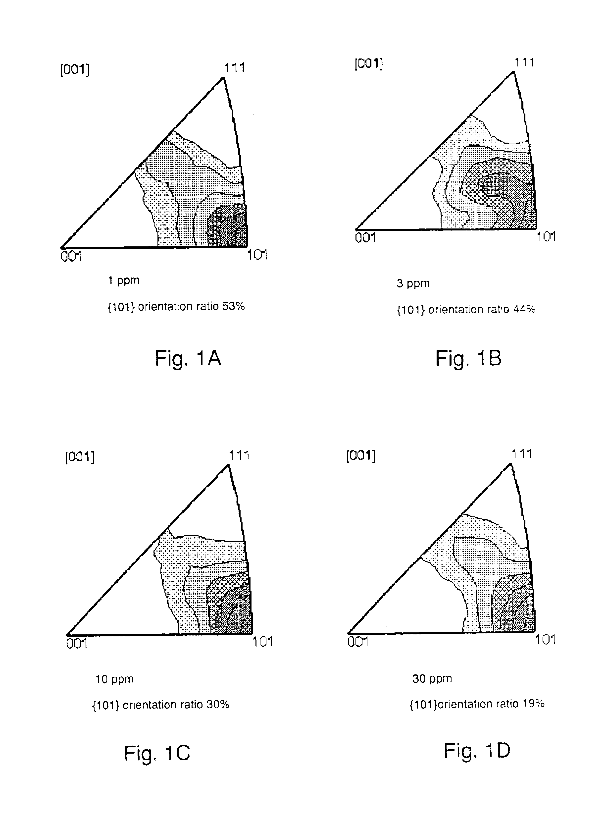
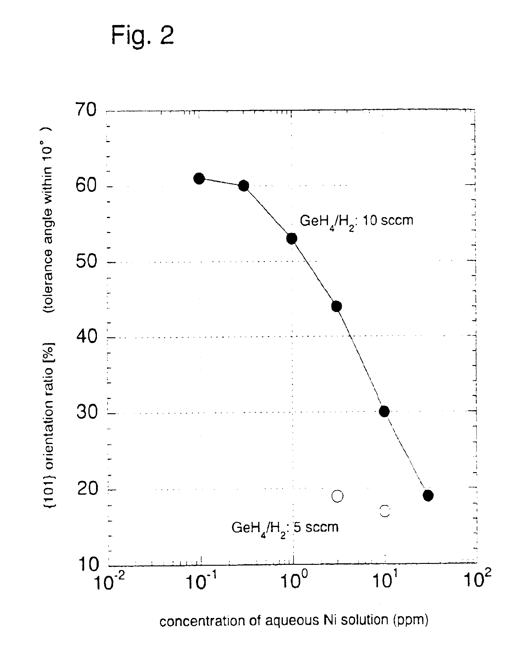
An amorphous silicon film 203 containing germanium is manufactured by plasma CVD, and is formed on the substrate 201 by introducing SiH.sub.4 and GeH.sub.4 gas diluted to 10% by SiH.sub.4 and H.sub.2, into a reaction chamber and performing glow discharge sepa...

embodiment mode 2

[Embodiment Mode 2]

A method of selectively forming a metal element for promoting crystallization of an amorphous semiconductor film is explained using FIG. 12A. A glass substrate as stated above, or a quartz substrate is employed as a substrate 220 in FIG. 12A. If a glass substrate is used, then a blocking layer is formed similar to that of embodiment mode 1.

An amorphous silicon film 221 containing germanium may be formed similar to that of embodiment mode 1 by plasma CVD, and germanium may be introduced by ion injection or ion doping. Further, it is also possible to employ a method of formation by low pressure CVD in which Si.sub.2 H.sub.6 and GeH.sub.4 are separated at a temperature of 450 to 500.degree. C.

A silicon oxide film 222 having a thickness of 150 nm is then formed on the amorphous silicon film 221 containing germanium. There are no particular limitations on the method of manufacturing the silicon oxide film, for example, it can be formed with a mixture of TEOS (tetraethy...

embodiment mode 3

[Embodiment Mode 3]

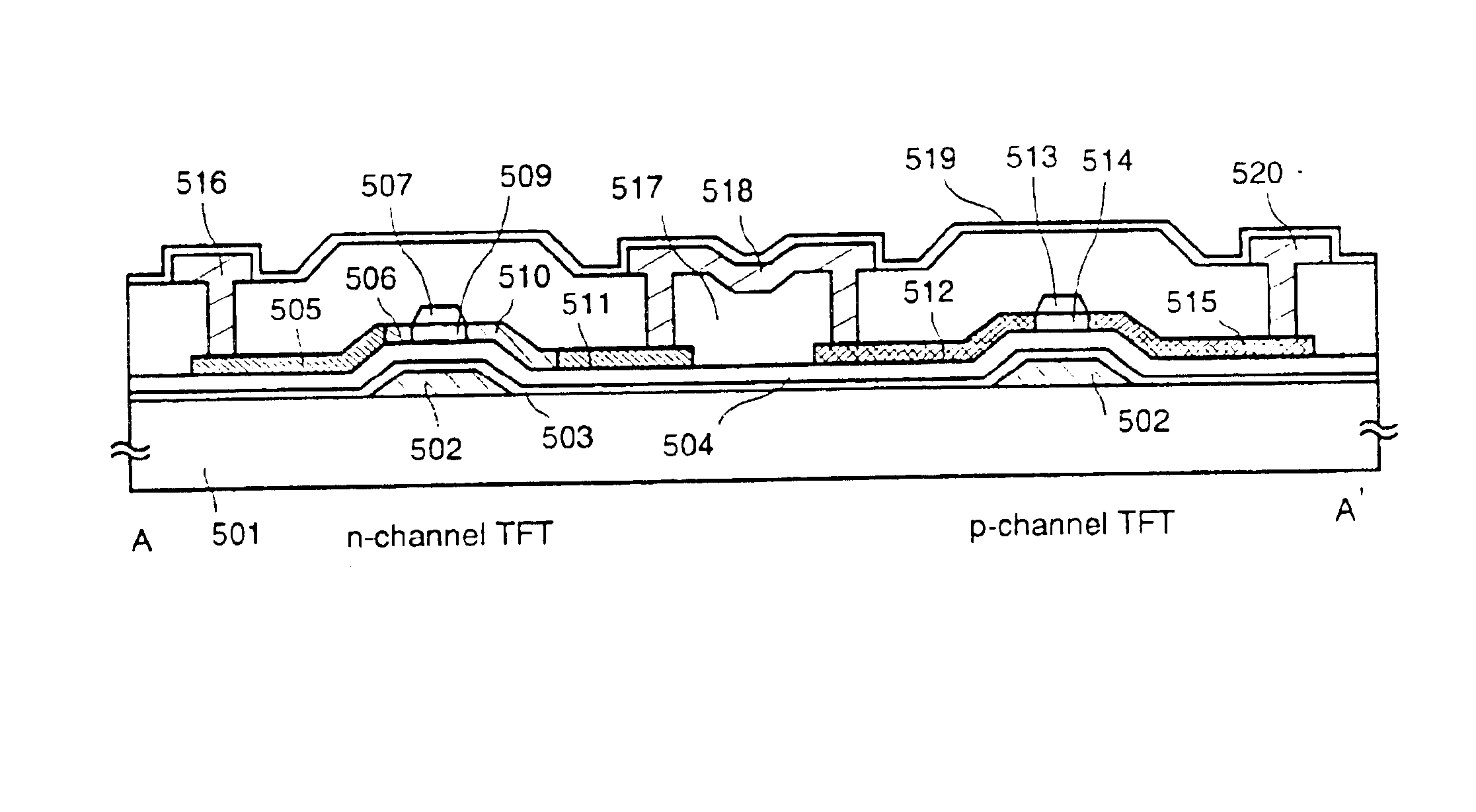
The metal element, utilized in crystallization of the crystalline silicon films manufactured in accordance with the methods explained by embodiment mode 1 and embodiment mode 2, remains after crystallization. Even if the metal element does not have a uniform distribution within the film, it exists at an average concentration exceeding 1.times.10.sup.19 / cm.sup.3. It is of course possible to use the film in this state in a channel-forming region for all types of semiconductor devices including TFTs, but it is preferable to remove the metal element by gettering.

One example of a gettering method is explained in embodiment mode 3 using FIGS. 12B-a to 12B-c. A glass substrate or a quartz substrate is employed as a substrate 230 in FIG. 12B-a. If a glass substrate is used, a blocking layer similar to that of embodiment mode 1 is formed. A silicon oxide film 232 is formed with a thickness of 150 nm as a mask on the surface of a crystalline semiconductor film 231, and an ...


PUM

PropertyMeasurementUnit
diameteraaaaaaaaaa
thicknessaaaaaaaaaa
thicknessaaaaaaaaaa

Abstract

Crystal orientation planes exist randomly in a crystalline silicon film manufactured by a conventional method, and the orientation ratio is low with respect to a specific crystal orientation. A semiconductor film having a high orientation ratio for the {101} lattice plane is obtained if crystallization of an amorphous semiconductor film, which has silicon as its main constituent and contains from 0.1 to 10 atom % germanium, is performed after introduction of a metal element. A TFT is manufactured utilizing the semiconductor film.

Description

1. Field of the InventionThe present invention relates to a semiconductor device in which an active region is formed by a semiconductor film having a crystalline structure. In particular, the present invention relates to a semiconductor device in which a thin film transistor is formed, or in which a circuit is formed by thin film transistors. Note that, in this specification, the term semiconductor device indicates general devices which can function by utilizing semiconductor characteristics, and that semiconductor integrated circuits, electro-optical devices, and electronic devices are all included in the category of semiconductor devices.Note also that, throughout this specification, the term semiconductor device indicates general devices which can function by utilizing semiconductor characteristics, and electro-optical devices, semiconductor circuits, and electronic devices are all semiconductor devices.2. Description of the Related ArtTechniques of using a semiconductor film (he...

Claims


Application Information

Patent Timeline
Patent Type & Authority Patents(United States)
IPC IPC(8): H01L21/20H01L29/66H01L21/02H01L21/336H01L21/70H01L27/12H01L29/786H01L21/84H01L21/77H01L27/13H01L29/04
CPCH01L21/2022H01L21/2026H01L27/1266H01L27/1277H01L29/66757H01L29/78684H01L27/1255H01L29/045H01L21/02488H01L21/02422H01L21/02395H01L21/02609H01L21/0242H01L21/02672H01L21/02686H01L21/02678H01L21/02532H01L21/02381H01L21/02691
Inventor YAMAZAKI, SHUNPEIMITSUKI, TORUKASAHARA, KENJIASAMI, TAKETOMITAKANO, TAMAESHICHI, TAKESHIKOKUBO, CHIHO
Owner SEMICON ENERGY LAB CO LTD
Why Eureka
Try Eureka