Pellicle and method for producing pellicle

a technology of pellicle and euv, which is applied in the field of pellicle for lithography, can solve the problems of many technical problems which have to be solved for realization of pellicle for euv, pattern width of 32 nm or less, and difficulty in meeting patterning requiring further miniaturization, etc., and achieves stably performed, improved cleavage resistance and chemical stability, and increased strength.

Active Publication Date: 2009-11-26
SHIN ETSU CHEM IND CO LTD
View PDF8 Cites 17 Cited by
  • Summary
  • Abstract
  • Description
  • Claims
  • Application Information

AI Technical Summary

Benefits of technology

[0024]In the present invention, the pellicle film and a base substrate supporting the pellicle film are formed of a single substrate, and the base substrate is provided with an opening whose ratio in area to an exposure region when the pellicle is used on a photomask (an open area ratio) is 60% or more, and provided with a reinforcing frame in a non-exposure region of the base substrate, and therefore, an integrated structure of the pellicle film and the base substrate is obtained, and the strength thereof can be increased by the reinforcing frame. Moreover, a principal plane of a silicon single crystal film is a crystal plane inclined at 3 to 5° from any lattice plane belonging to {100} planes or {111} planes, and therefore

Problems solved by technology

However, in such lithography based on the excimer exposure technologies, it is regarded as difficult to meet patterning requiring further miniaturization with a pattern width of 32 nm or less.
Among these, development for the light source and resist has been already made substantial progress, whereas for pellicle, many technical problems which have to be solved for realization of a pellicle for EUV remain unsolved.
However, the prospects for resolution of problems of such high transmission and chemical stability, and further the material development for a practical pellicle film having an excellent fabrication yield are still far from certain at present.
However, silicon used as a pellicle film in Non-Patent Document 1 is a film deposited by a sputtering method or the like, and therefore necessarily become amorphous, inevitably resulting in the high absorption coefficient and low transmittance in the EUV region.
In addition, there are also the following problems: as the pellicle films disclosed in Patent Document 1 and Non-Patent Document 1, a strong stress is easily introduced into a silicon crystal formed by a sputtering or CVD

Method used


Image

  • Pellicle and method for producing pellicle
  • Pellicle and method for producing pellicle
  • Pellicle and method for producing pellicle

Examples


example 1

[0066]FIGS. 3A to 3D are views for explaining a process example of a method for producing a pellicle of the present invention. In the case where SOI substrates in a broad sense are an SOQ (Silicon On Quartz) substrate and an SOG (Silicon On Glass) substrate, support substrates (base substrates) thereof were a quartz substrate and a glass substrate, respectively. A support substrate of an SOI (Silicon On Insulator) substrate in a limited sense was a substrate provided with an oxide film on a silicon substrate surface.

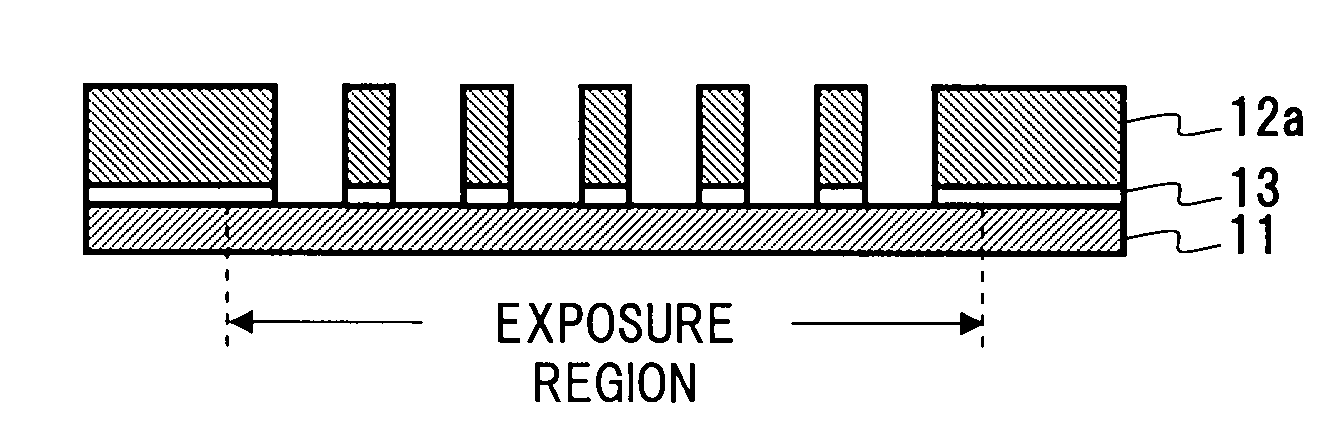
[0067]In FIGS. 3A to 3D, an example using the SOI substrate in a limited sense is illustrated, in which a silicon single crystal film 11 was provided on one principal plane of a support substrate (a base substrate) 12 via an oxide film 13 (FIG. 3A).

[0068]For the reason above-mentioned, the silicon single crystal film 11 was a film having a crystal plane as its principal plane, the crystal plane being inclined at 3 to 5° from a lattice plane belonging to {111} planes, the...

example 2

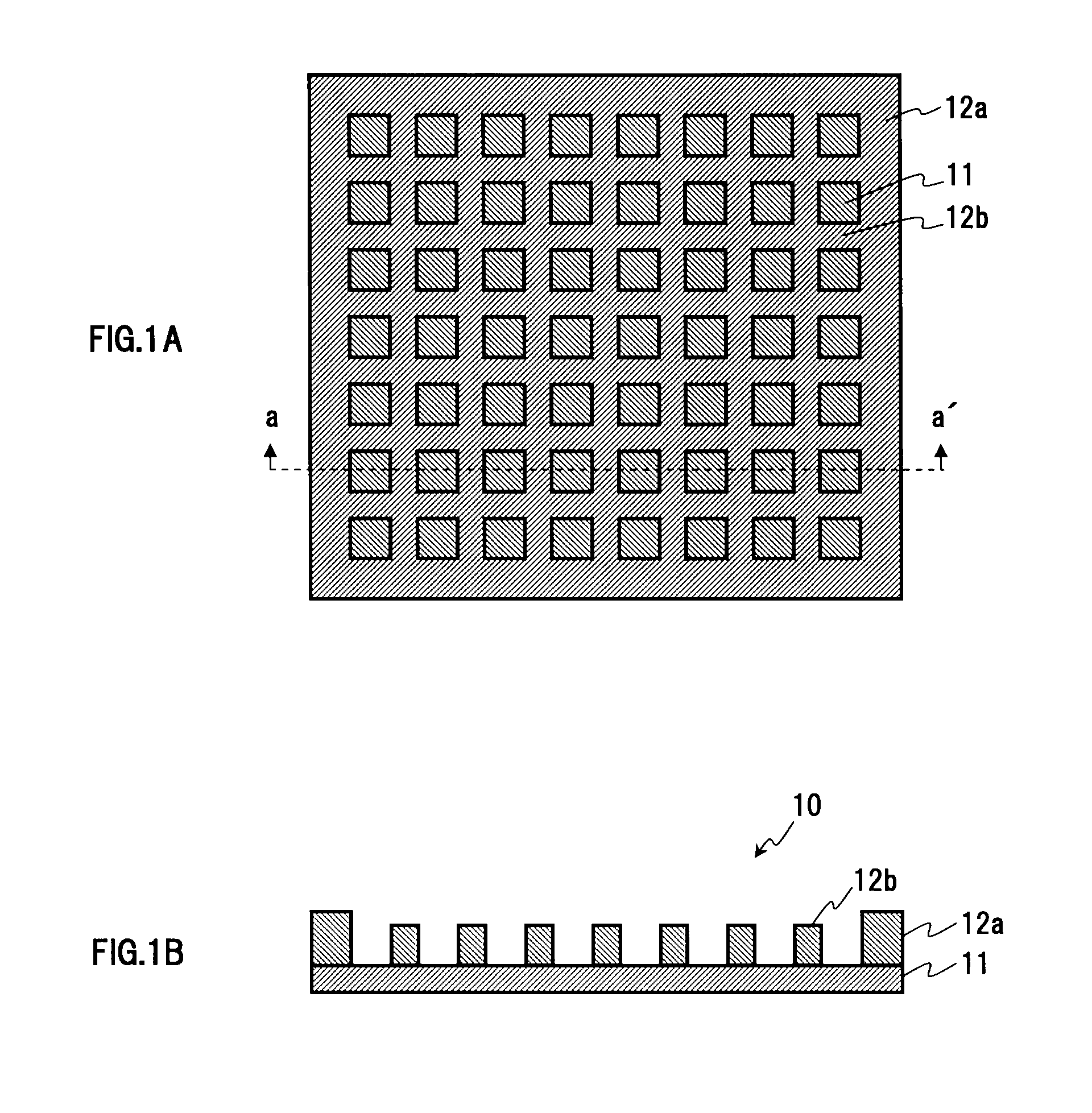
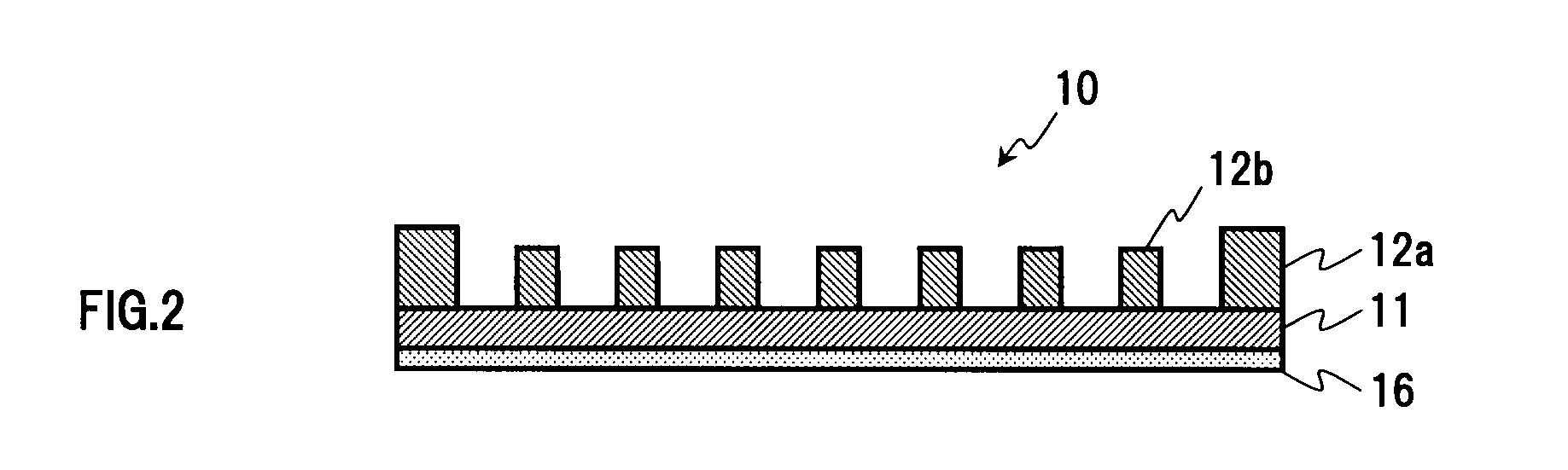
[0080]As described in EXAMPLE 1, the silicon substrate 12, which is the support substrate (the base substrate) of the SOI substrate, was subjected to a counterbore by grinding and polishing to about 150 μm, the reinforcing frame was formed by leaving the outermost periphery width of 5 mm, the oxide film 13 was exposed by etching a silicon section made thin in an exposed area into a window frame shape by KOH etchant such that the open area ratio was 75%, and thereafter the oxide film 13 was also removed by HF to leave only the silicon single crystal film 11, thereby forming the pellicle film.

[0081]A silicon single crystal having an orientation plane as its principal plane was used, the orientation plane with a crystal orientation of a silicon single crystal film inclined at 3 to 5° (3°-off to 5°-off) from to direction. Subsequently, this was bonded to the pellicle frame 12. The pellicle film 11 of the silicon single crystal film of the EXAMPLE had a thickness of 20 nm.

[0082]Then, o...


PUM


Abstract

A pellicle film of a silicon single crystal film and a base substrate supporting the pellicle film are formed of a single substrate using an SOI substrate. The base substrate is provided with an opening whose ratio in area to an exposure region when a pellicle is used on a photomask (an open area ratio) is 60% or more, and provided with a reinforcing frame in a non-exposure region of the base substrate. Since the pellicle film and the base substrate supporting the pellicle film are formed of the single substrate (an integrated structure), and the base substrate is provided with the reinforcing frame, the effect of increased strength is obtained. Moreover, a principal plane of a silicon single crystal film is a crystal plane inclined at 3 to 5° from any lattice plane belonging to {100} planes or {111} planes.

Description

[0001]This application claims priority from Japanese Patent Application No. 2008-134261 filed May 22, 2008, which is incorporated hereinto by reference in its entirely.BACKGROUND OF THE INVENTION[0002]1. Field of the Invention[0003]The present invention relates to a pellicle for lithography. More particularly, the present invention relates to a pellicle suitable for lithography using extreme ultra violet (EUV) light, and a method for producing the same.[0004]2. Description of the Related Art[0005]With high integration of semiconductor devices, patterns formed by lithography are microminiaturized, and currently devices having a pattern width of about 45 nm are being put to practical use. Such a narrow line pattern can be realized by lithography based on a manner such as an ArF immersion method and a double exposure method which are improved techniques of conventional excimer exposure technologies.[0006]However, in such lithography based on the excimer exposure technologies, it is reg...

Claims


Application Information

Patent Timeline
IPC IPC(8): G03F1/00G03F1/24G03F1/62G03F1/64
CPCG03F1/142G03F1/64G03F1/62
Inventor KUBOTA, YOSHIHIROAKIYAMA, SHOJISHINDO, TOSHIHIKO
Owner SHIN ETSU CHEM IND CO LTD
Why Eureka
Try Eureka