Semiconductor device

a semiconductor and film technology, applied in the field of semiconductor devices, can solve the problems of increasing energy consumption in the manufacturing process, difficult to say the method, and long treatment time in the proper method, and achieve the effect of improving the orientation of the crystalline semiconductor film

Inactive Publication Date: 2005-10-18
SEMICON ENERGY LAB CO LTD
View PDF37 Cites 17 Cited by
  • Summary
  • Abstract
  • Description
  • Claims
  • Application Information

AI Technical Summary

Benefits of technology

[0011]The present invention has been made to solve the above problems and an object of the present invention is to improve the orientation of a crystalline semiconductor film obtained by crystallizing an amorphous semiconductor film and to provide a TFT formed from the crystalline semiconductor film.
[0060]At this point, germanium does not react with this compound but causes local distortion by merely existing around the compound. The distortion increases the critical radius of nuclear generation and, overall, acts to reduce the nuclear generation density. The distortion also works to limit orientation of crystals.
[0062]When an amorphous semiconductor film is crystallized, atoms are rearranged so that the volume of the film is reduced macroscopically. As a result, tensile stress is generated in the crystalline semiconductor film formed on the substrate. However, if the amorphous semiconductor film is doped with 0.1 to 10 atomic percent, preferably 1 to 5 atomic percent, of germanium that has an atomic radius larger than that of silicon, the volume shrinkage accompanying crystallization is reduced and the tensile stress to be generated is accordingly reduced. In short, doping with germanium in a given concentration can ease distortion in the crystalline semiconductor film.

Problems solved by technology

Considering the productivity in manufacturing TFTs, it is difficult to say the method with the treatment temperature this high and the treatment time this long is a proper method.
This not only increases energy consumption in manufacturing process but also makes it difficult to obtain uniform crystals over the large surface area.
On the other hand, when laser treatment is chosen, obtaining crystals of uniform quality is still difficult because the output of a laser oscillator is not stable.
The diversity in quality between crystals results in fluctuation in characteristic between TFTs, which in turn causes lowering of display quality of the liquid crystal display device or a display device whose pixel portion is composed of light emitting elements.
However, a TFT manufactured by using the thus formed crystalline silicon film is still inferior in characteristics to a MOS transistor comprised of a single crystal silicon substrate.
In the polycrystalline structure, carriers are trapped by an infinite number of defects found in crystal grains and in grain boundaries to limit the performance of the TFT.
When the orientation ratio is low, it is nearly impossible to keep the continuity of lattice in the grain boundaries where crystals of different orientations meet, and hence many dangling bonds will presumably be generated.
Furthermore, grain boundaries are arranged at random, meaning that a channel formation region cannot be formed from crystal grains of a specific crystal orientation.
This can cause fluctuation in electric characteristics of TFTs.

Method used


Image

  • Semiconductor device
  • Semiconductor device
  • Semiconductor device

Examples


embodiment mode 1

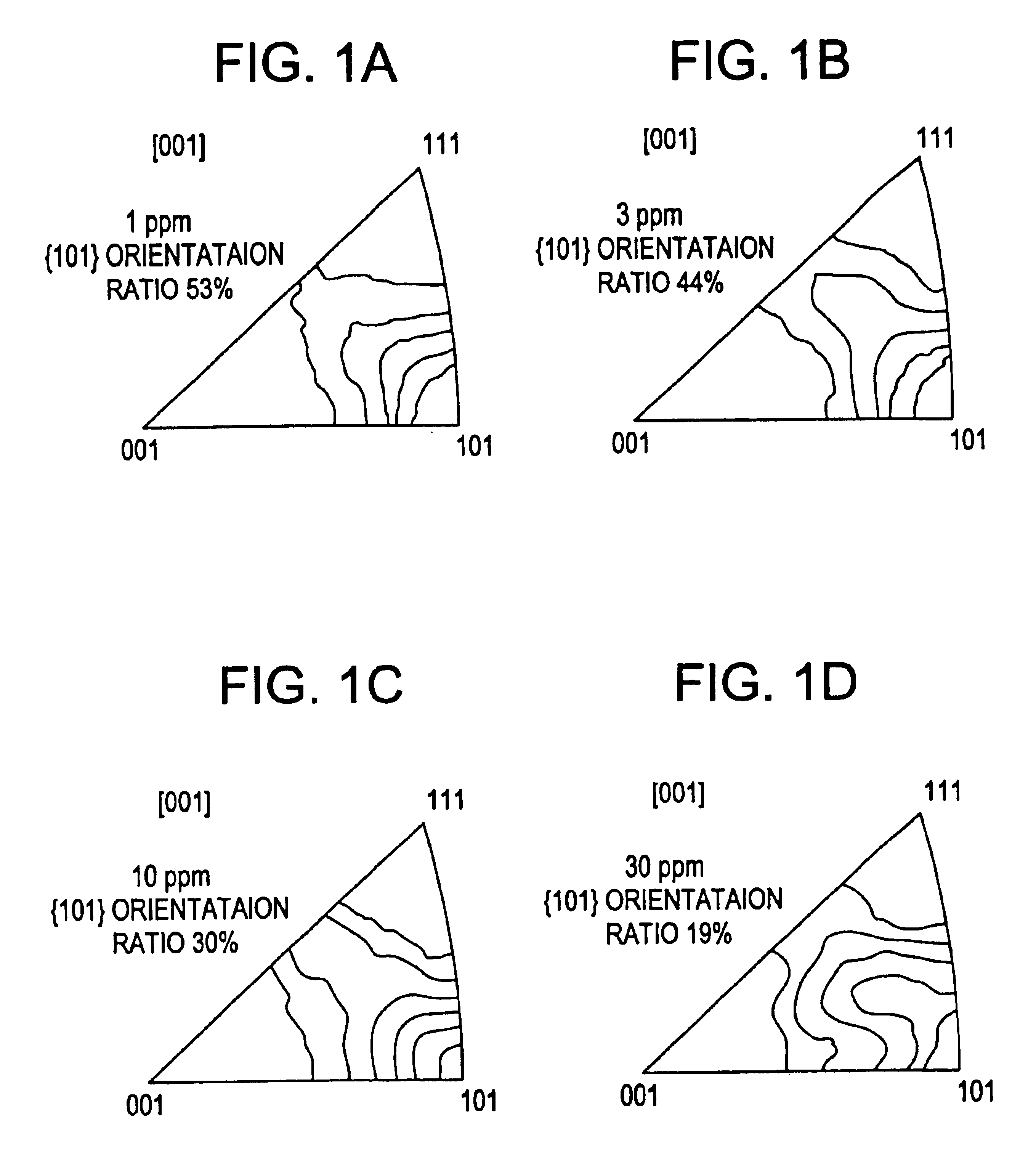
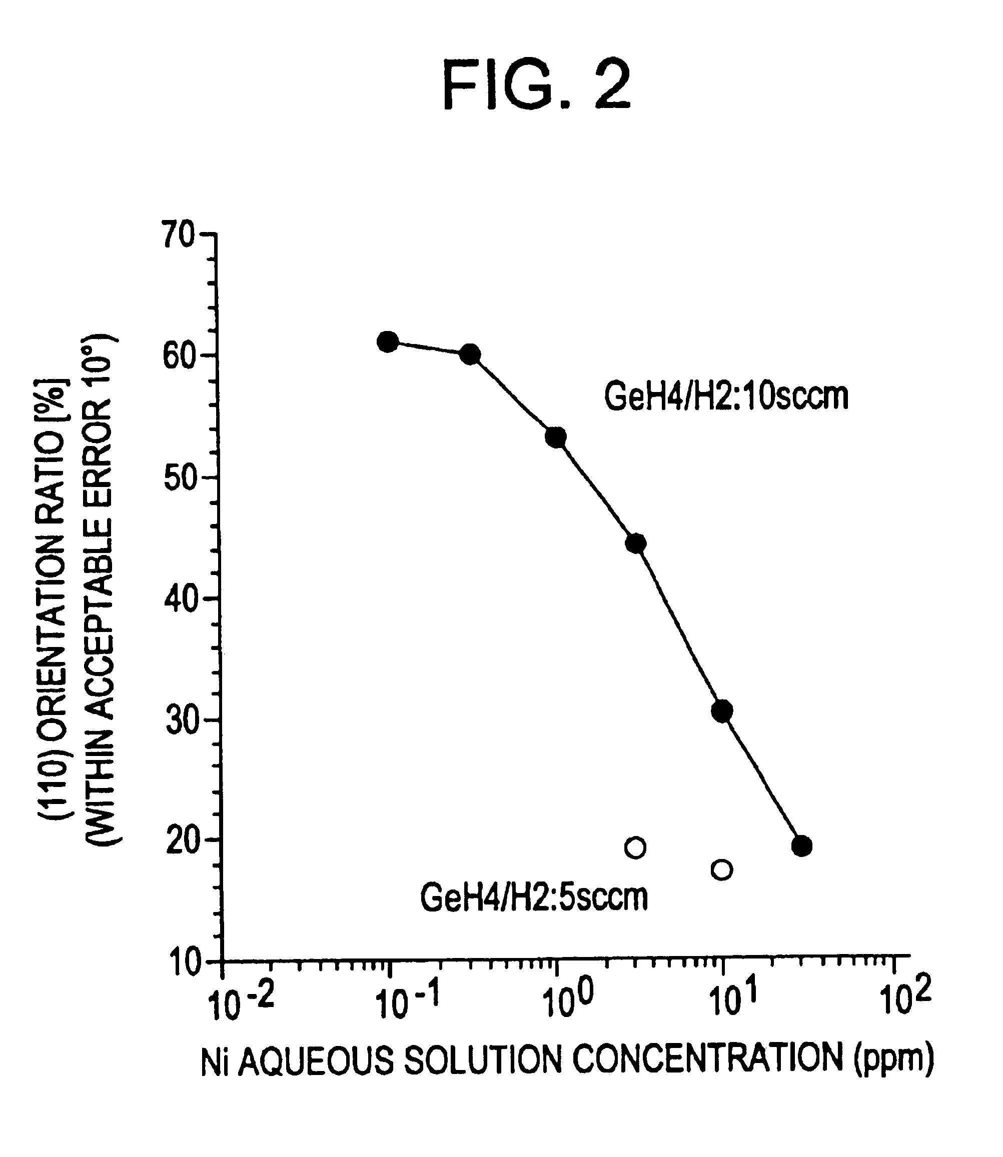
[0152]The method of manufacturing a crystalline semiconductor film in accordance with illustration of FIGS. 1A to 11D is to crystallize an amorphous silicon film containing germanium by doping the entire surface of the amorphous silicon film with a metal element for promoting crystallization of silicon. In FIG. 11A, a glass substrate, typically, the Corning #1773 glass substrate (product of Corning Incorporated), is used for a substrate 201. On the surface of the substrate 201, a silicon oxynitride film is formed as a blocking layer 202 from SiH4 and N2O by plasma CVD to a thickness of 100 nm. The blocking layer 202 is provided to prevent an alkaline metal contained in the substrate from diffusing into a semiconductor film to be formed on the blocking layer.

[0153]An amorphous silicon film 203 containing germanium is formed by plasma CVD. SiH4 gas and GeH4 gas which is diluted by H2 to 10% is introduced in a reaction chamber and decomposed by glow discharge to be deposited on the sub...

embodiment mode 2

[0157]A method of selectively introducing a metal element for promoting crystallization of an amorphous semiconductor film will be described with reference to FIGS. 12A to 12C. In FIG. 12A, a substrate 220 may be the aforementioned glass substrate or a quartz substrate. When the glass substrate is employed, a blocking layer is formed as in Embodiment Mode 1.

[0158]An amorphous silicon film 221 containing germanium may be formed by plasma CVD as in Embodiment Mode 1, or by introducing germanium through ion implantation or ion doping. The film may also be formed by low pressure CVD in which Si2H6 and GeH4 are decomposed at a temperature of 450 to 500° C.

[0159]A silicon oxide film 222 with a thickness of 150 nm is formed on the amorphous silicon film 221 containing germanium. The method of forming the silicon oxide film is not limited. For example, the film is formed through discharge in which a mixture of tetraethyl ortho silicate (TEOS) and O2 is used, and the reaction pressure is set...

embodiment mode 3

[0162]The crystalline silicon film formed in accordance with the method described in Embodiment Mode 1 or 2 still has the metal element that has been utilized in crystallization. Although not distributed in the film uniformly, the metal element remains in a concentration over 1×10¹⁹ atoms / cm3 on the average. The film in this state can be used for a channel formation region of a TFT and other various semiconductor devices, of course, but it is preferred to remove the metal element from the film by gettering.

[0163]An example of the gettering method according to this embodiment mode will be described with reference to FIGS. 13A to 13C. In FIG. 13A, the glass substrate of Embodiment Mode 1 or a quartz substrate is employed as a substrate 230. When the glass substrate is used, a blocking layer is formed similar to Embodiment Mode 1. A crystalline silicon film 231 can be formed by the method described in Embodiment Mode 1 or the method described in Embodiment Mode 2. On the surface of the...


PUM

PropertyMeasurementUnit
angleaaaaaaaaaa
temperatureaaaaaaaaaa
angleaaaaaaaaaa

Abstract

The orientation of a crystalline semiconductor film obtained by crystallizing an amorphous semiconductor film is improved and a TFT formed from this crystalline semiconductor film is provided. In a semiconductor device whose TFT is formed from a semiconductor layer mainly containing silicon, the semiconductor layer has a channel formation region and an impurity region doped with an impurity of one type of conductivity. 20% or more of the channel formation region is the {101} lattice plane that forms an angle of equal to or less than 10 degree with respect to the surface of the crystalline semiconductor film, the plane being detected by an electron backscatter diffraction pattern method, 3% or less of the channel formation region is the {001} lattice plane that forms an angle of equal to or less than 10 degree with respect to the surface of the crystalline semiconductor film, 5% or less of the channel formation region is the {111} lattice plane that forms an angle of equal to or less than 10 degree with respect to the surface of the crystalline semiconductor film.

Description

BACKGROUND OF THE INVENTION[0001]1. Field of the Invention[0002]The present invention relates to a semiconductor device whose active region is formed from a semiconductor film constituted of a mass of crystals with various orientations (the film hereinafter is referred to as crystalline semiconductor film). Typical example of the crystalline semiconductor film is a polycrystalline silicon film. Specifically, the invention relates to a thin film transistor or a semiconductor device that has a circuit composed of the thin film transistor. The term semiconductor device herein refers to a device in general which utilizes semiconductor characteristics to function, and semiconductor integrated circuits, electro-optical devices and electronic equipment fall within this category.[0003]2. Description of the Related Art[0004]A technique has been developed to manufacture a thin film transistor (hereinafter referred to as TFT) from a crystalline semiconductor film with a thickness of several nm...

Claims


Application Information

Patent Timeline
Patent Type & Authority Patents(United States)
IPC IPC(8): H01L21/336H01L29/786H01L21/70H01L29/04H01L29/40H01L29/66H01L21/02H01L29/423H01L29/02H01L29/49H01L27/12H01L21/84G02F1/13G02F1/1362G02F1/1368G09F9/30G09F9/35H01L21/20H01L21/28H01L21/77H01L21/8238H01L27/08H01L27/092
CPCH01L27/12H01L29/045H01L29/42384H01L29/4908H01L29/66757H01L29/78624H01L29/78675H01L29/78684H01L29/78696H01L27/1277G02F1/13454
Inventor YAMAZAKI, SHUNPEIMITSUKI, TORUKASAHARA, KENJIASAMI, TAKETOMITAKANO, TAMAESHICHI, TAKESHIKOKUBO, CHIHO
Owner SEMICON ENERGY LAB CO LTD
Why Eureka
Try Eureka