Optical waveguide and fabrication method

a fabrication method and waveguide technology, applied in the field of fabrication of optical waveguides, can solve the problems of inconvenient arrangement for many waveguide applications or as a single-mode waveguid

Inactive Publication Date: 2004-12-21
QINETIQ LTD
View PDF21 Cites 5 Cited by
  • Summary
  • Abstract
  • Description
  • Claims
  • Application Information

AI Technical Summary

Problems solved by technology

While this provided a bulk guiding structure, the large lateral dimension of the flat "core" lamina meant that the arrangement was not useful for many waveguiding applications or as a single-mode waveguide.

Method used


Image

  • Optical waveguide and fabrication method
  • Optical waveguide and fabrication method
  • Optical waveguide and fabrication method

Examples


first embodiment

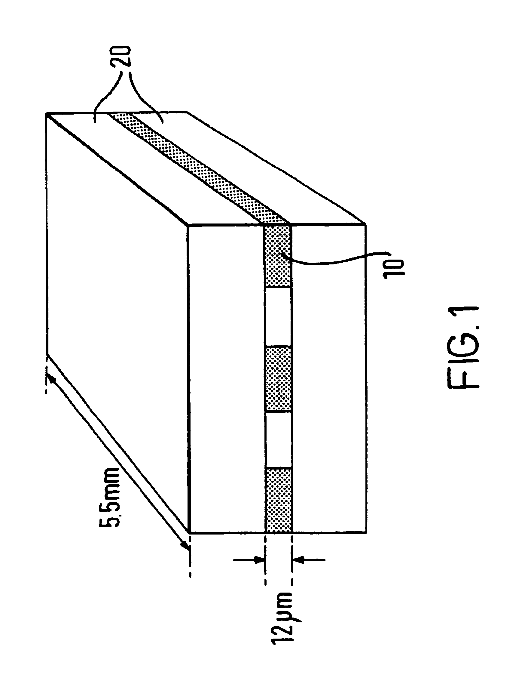
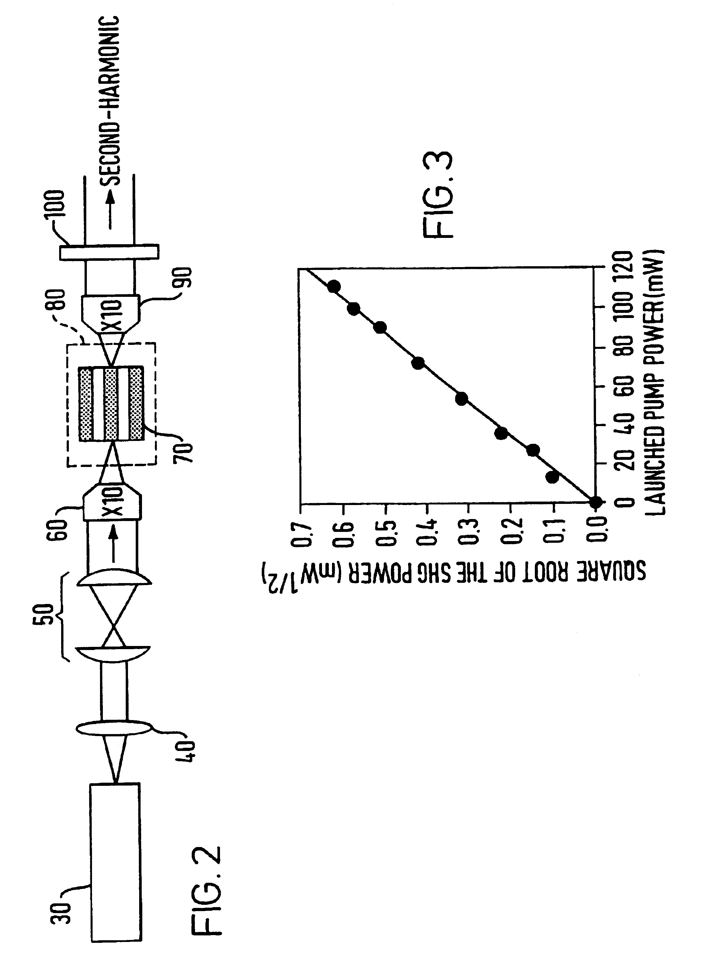
In summary, for the invention these experiments demonstrate the successful prototype fabrication of a 12-.mu.m-thick, 5.5-mm-long, symmetrical PPLN waveguide buried in LiNbO.sub.3 by DB. Using the 6.50-.mu.m-period PPLN grating at an elevated temperature of 174.degree. C., an efficient quasi-phase-matched frequency doubling of the 1064 nm line of a cw diode-pumped Nd:YAG laser has been demonstrated. For 204 mW of fundamental pump power, nearly 2 mW of green power was generated at an output wavelength of 532 nm. This result was obtained with non-optimum focusing conditions but remains higher than the theoretical expectation for a similar length of bulk material. The waveguiding properties were shown to be different in the PPLN, and unpoled LiNbO.sub.3 regions of the sample, with the PPLN section showing a surprising single-spatial-mode behaviour. These results suggest that the production of longer buried waveguides, potentially incorporating channel structures, should lead to highly-...

second embodiment

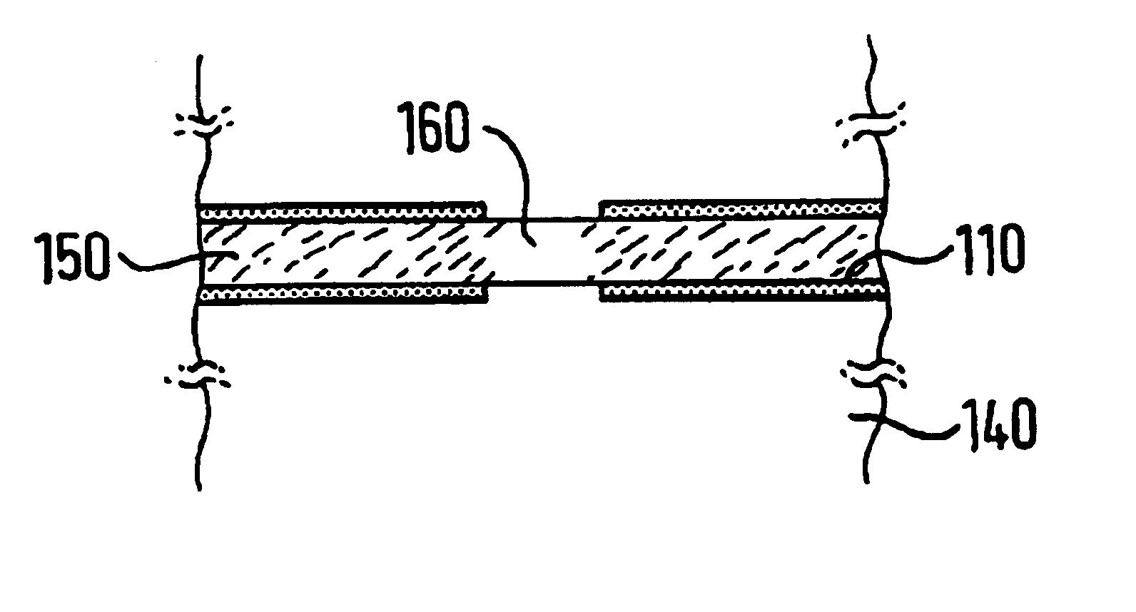
Referring now to FIGS. 4 and 5, a second embodiment using an indiffusion technique to define a waveguide path will be described.

In this second embodiment, a piece of PPLN 100 is made by the conventional electrical poling method. The piece 100 might be, for example, 500 .mu.m thick and several mm in the other two dimensions. One face 110 of the piece 100 is patterned with magnesium oxide (using a process of photolithography and vacuum evaporation or sputtering). The magnesium oxide lamina is less than about 400 nm thick, and defines (by the parts not covered by the lamina) a waveguide path along the piece 100. The piece 100 is then heated to a temperature of between about 600.degree. C. and about 1200.degree. C. This causes the magnesium oxide material to diffuse in and, in the indiffused regions 130, locally lower the refractive index.

The piece 100 is then bonded, by a direct bonding process applied to the face 110, to a LiTaO.sub.3 substrate (140, FIG. 5), before being polished dow...


PUM

PropertyMeasurementUnit
phase-matching temperatureaaaaaaaaaa
wavelengthaaaaaaaaaa
thickaaaaaaaaaa

Abstract

An optical waveguide with at least a guiding lamina (10) of optical material bonded by direct interfacial bonding to a superstructure lamina (20) of optical material, in which regions of the guiding lamina have modified optical properties so as to define a light guiding path along the guiding lamina. In a particular example, a periodically poled LiNbO3 planar waveguide is buried in LiTaO3 by direct interfacial bonding and precision polishing techniques and used in an optical frequency doubling system.

Description

This application is the US national phase of International Application No. PCT / GB99 / 03055, filed 14 Sep. 1999, which designated the U.S., the entire content of which is hereby incorporated by reference.1. Field of the InventionThis invention relates to the fabrication of optical waveguides.2. Discussion of Prior ArtOne known technique for fabricating optical waveguides is the so-called direct bonding (or direct interfacial bonding) technique.Direct bonding (DB) is a fabrication technique that uses the Van der Waals forces present when two atomically flat bodies approach each other to create a bond between two bodies. If the bodies are laminas of optical material having appropriate refractive indices, the material laminas can be joined to form waveguiding boundaries.In one established way to form such a bond the surfaces of two pieces of optical material are polished so as to be very flat (i.e. substantially flat at atomic dimensions). The crystalline structures of the two polished f...

Claims


Application Information

Patent Timeline
Patent Type & Authority Patents(United States)
IPC IPC(8): G02B6/13G02F1/39G02F1/377G02B6/12G02B6/134G02F1/35G02F1/355
CPCG02B6/12G02B6/1342G02F1/377G02F1/395G02F1/3558G02F2202/20G02F2201/15G02F2202/07G02F1/3775
Inventor SMITH, PETER G RROSS, GRAEME WHANNA, DAVID CSHEPHERD, DAVID PGAWITH, CORIN B E
Owner QINETIQ LTD
Why Eureka
Try Eureka