Substrate processing method and substrate processing apparatus

a substrate processing and substrate technology, applied in the direction of photomechanical equipment, instruments, photosensitive materials, etc., can solve the problems of the line width of resist patterns of the late years is remarkably small, and achieve the effect of preventing pattern deformation or breaking

Inactive Publication Date: 2005-01-04
TOKYO ELECTRON LTD
View PDF7 Cites 28 Cited by
  • Summary
  • Abstract
  • Description
  • Claims
  • Application Information

AI Technical Summary

Benefits of technology

An object of the present invention is to provide a substrate processing method and a substra

Problems solved by technology

Line width of the resist patterns of the late years tends to be remarkably minute as technology advances.
However, because the line width of the resist patterns are too minute, especially w

Method used


Image

  • Substrate processing method and substrate processing apparatus
  • Substrate processing method and substrate processing apparatus
  • Substrate processing method and substrate processing apparatus

Examples


Embodiment Construction

Hereinafter, embodiments of the present invention will be described with reference to the drawings.

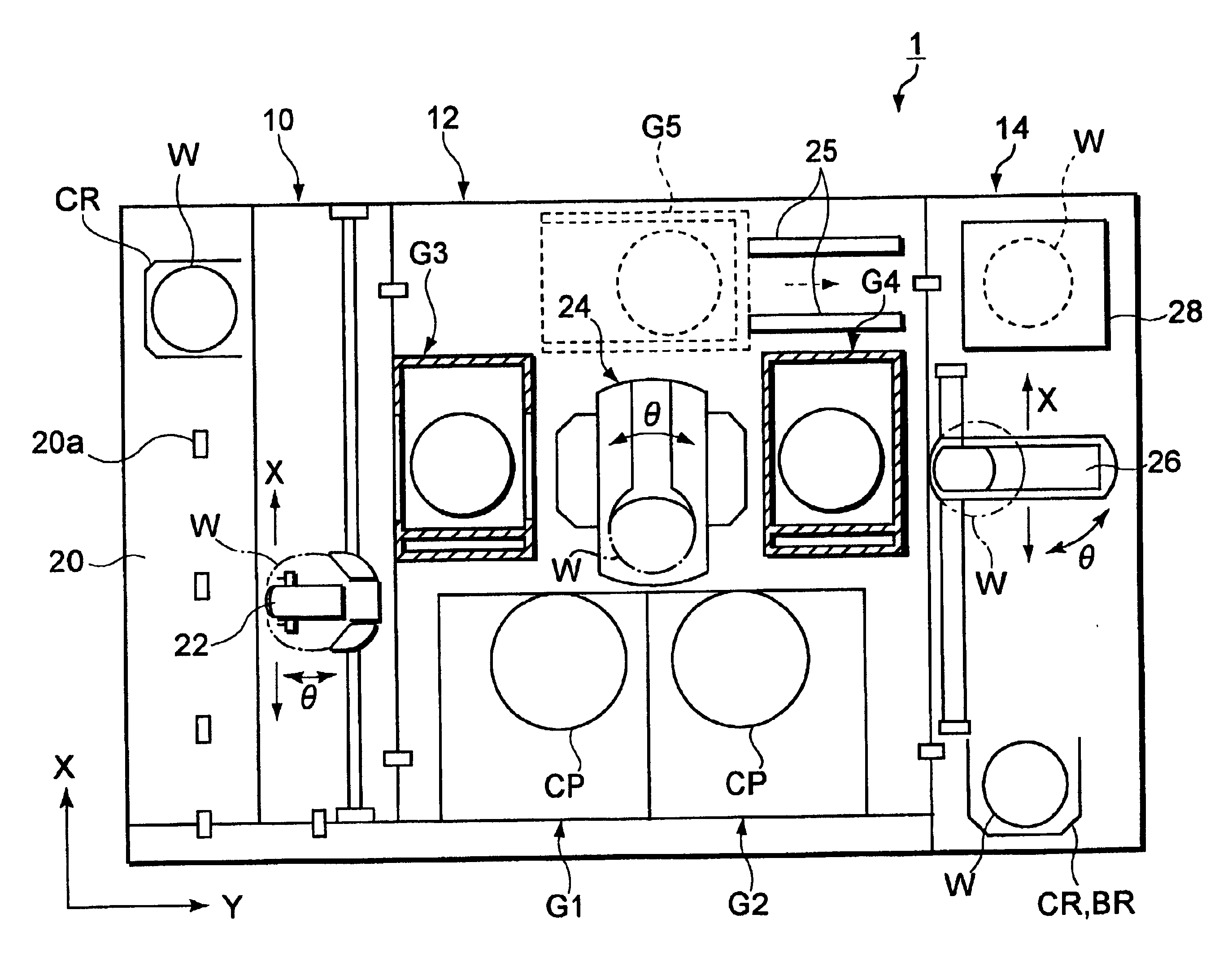
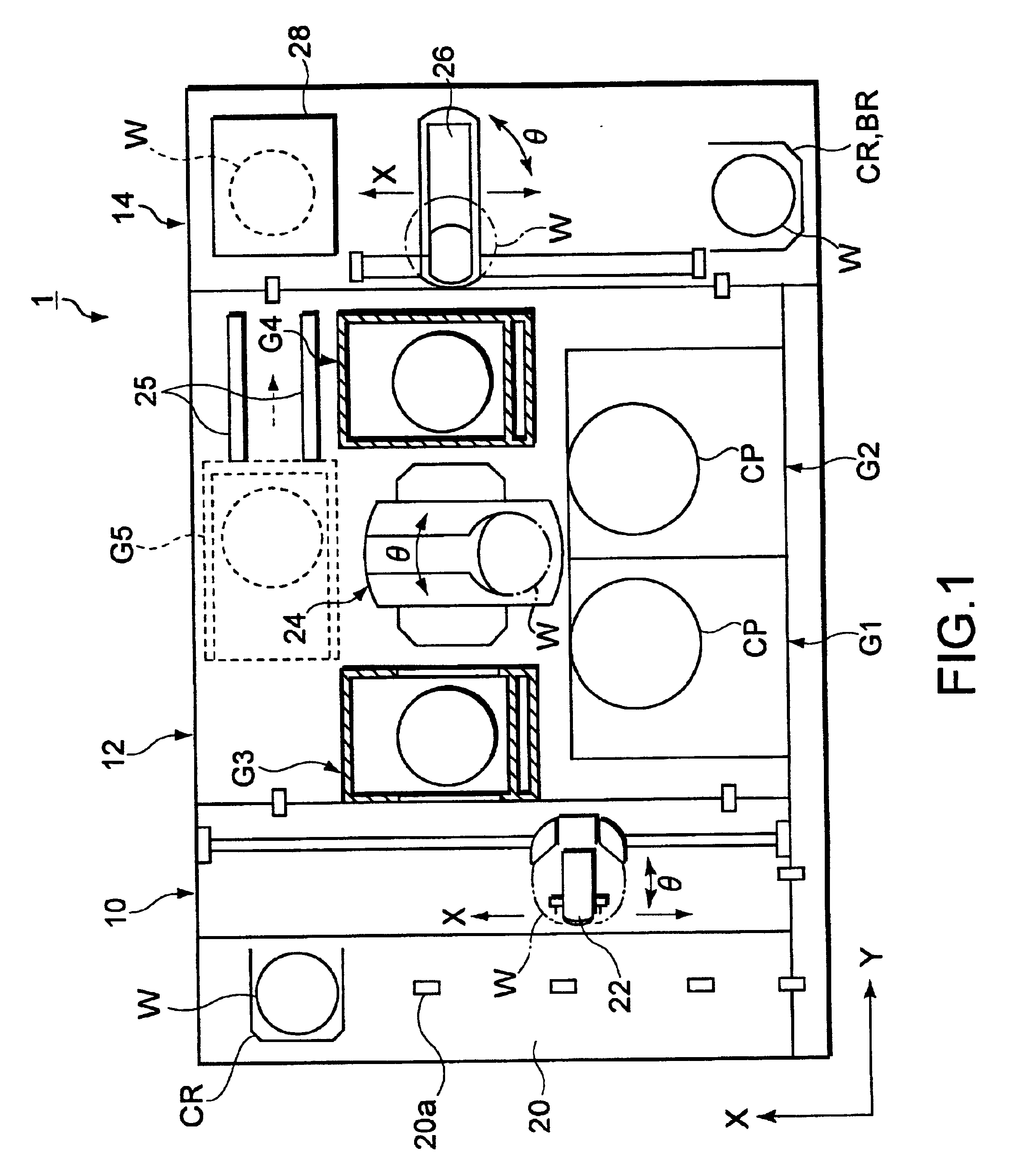
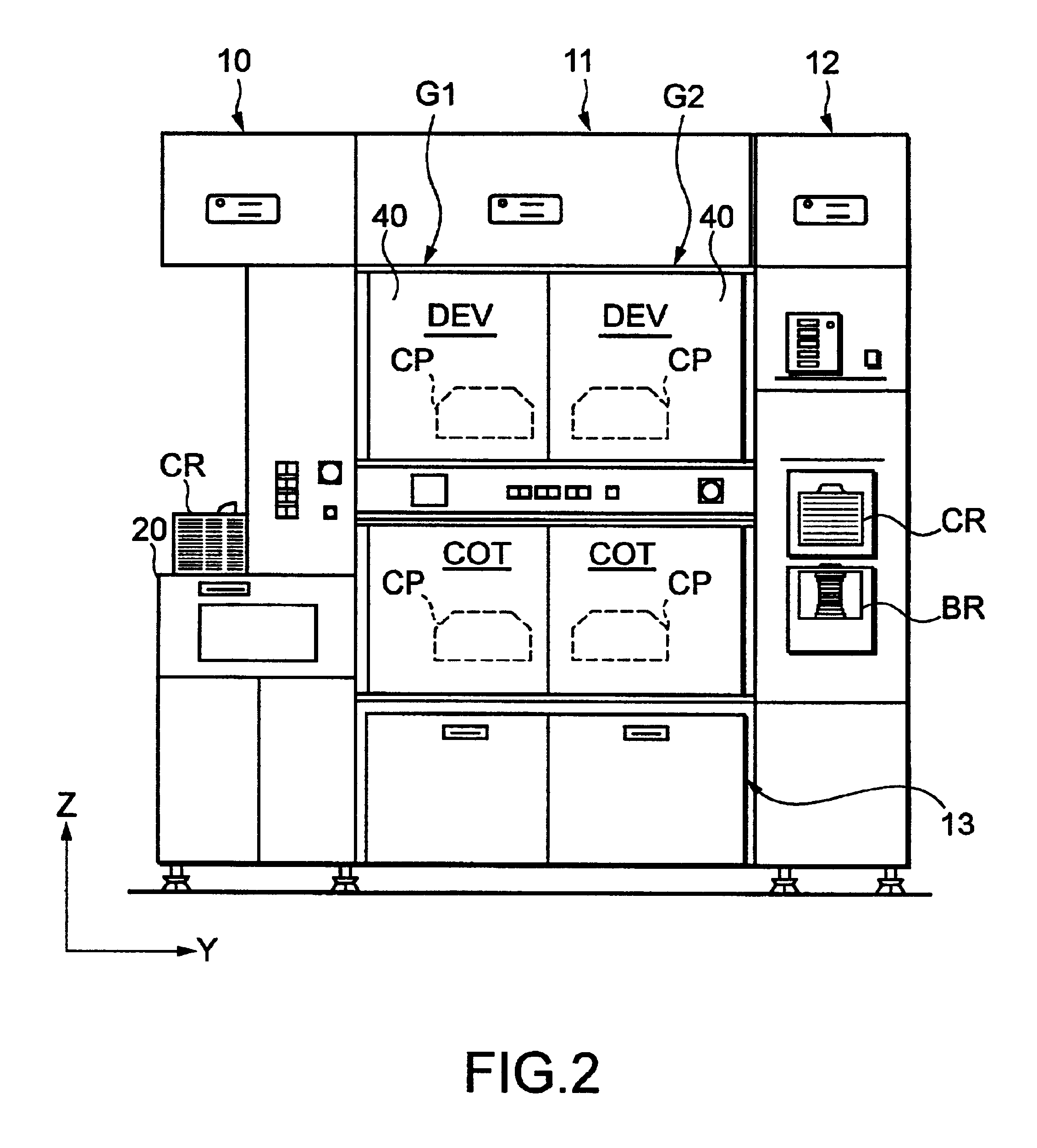
FIGS. 1, 2 and 3 are the views showing a total configuration of a substrate processing apparatus in an embodiment of the present invention. FIG. 1 is a plan view, FIG. 2 is a front view and FIG. 3 is a rear view.

A coating and developing system 1 is comprised of a cassette station 10 for carrying a plurality of, for example, 25 semiconductor wafers per a wafer cassette CR as a unit, into or out of the system from or to an outside, and carrying the wafer w in and out of the wafer cassette CR, a processing station 12 constituted by stacking various kinds of processing stations each for performing predetermined processing for the wafers W one by one in the resist coating process at predetermined locations in multiple tiers, an aligner provided adjacent to the processing station 12 (not shown) and a interface section 14 for transferring wafer W are integrally connected.

In the cassette stati...


PUM

PropertyMeasurementUnit
Timeaaaaaaaaaa
Pressureaaaaaaaaaa
Surfaceaaaaaaaaaa

Abstract

A developing process of the photo-resist coated on the wafer is performed, cleaning the developing solution by a cleaning solution then transferring the wafer to the electron beam radiation unit before the rinsing solution and the resist dries out. The radiation chamber is replaced with a helium gas to form a predetermined degree of vacuum or atmospheric pressure. An electron beam is radiated and the front face of the wafer is heated for a predetermined period of time. In this method, deformation and breaking of a pattern caused by drying after the development can be prevented.

Description

BACKGROUND OF THE INVENTION1. Field of the InventionThe present invention relates to a substrate processing method and a substrate processing apparatus for reforming a coating film by radiating a semi-conductor wafer with a beam.2. Description of the Related ArtIn a photolithography step of a semiconductor device manufacture, photo-resist is applied on the surface of a semi-conductor wafer (a resist application step) after printing mask patterns on the resist surface (an exposure step), a photo sensitive portion of the resist or a photo insensitive portion thereof is dissolved in developing solution selectively and the developing solution is washed away by rinsing solution (a development step) to form the resist patterns on the front face of a wafer. Line width of the resist patterns of the late years tends to be remarkably minute as technology advances.However, because the line width of the resist patterns are too minute, especially when aspect ratio is high, hardness of the resist...

Claims


Application Information

Patent Timeline
IPC IPC(8): G03F7/40G03F7/20G03F7/30H01L21/027
CPCG03F7/40G03F7/2024G03F7/3021H01L21/027
Inventor NAKANO, MASAYUKIDEGUCHI, YOICHI
Owner TOKYO ELECTRON LTD
Why Eureka
Try Eureka