Laser machining of semiconductor materials

Inactive Publication Date: 2005-01-11
XSIL TECH
View PDF11 Cites 57 Cited by
  • Summary
  • Abstract
  • Description
  • Claims
  • Application Information

AI Technical Summary

Benefits of technology

In one embodiment, the method comprises the further step of capturing an image of the material before

Problems solved by technology

Although this is the accepted technique there are problems with the use of such saws as they cause chipping, debris generation and excessive thermal loading.
Although laser processing and the use of lasers in manufacturing is widespread, laser technology does not appear to have been applied successfully to the machining of semiconductor materials and other similar applications.
T

Method used


Image

  • Laser machining of semiconductor materials
  • Laser machining of semiconductor materials
  • Laser machining of semiconductor materials

Examples


example 1

Machining a 700 μm Silicon Wafer with Two Laser Wavelengths in a Dual Headed System

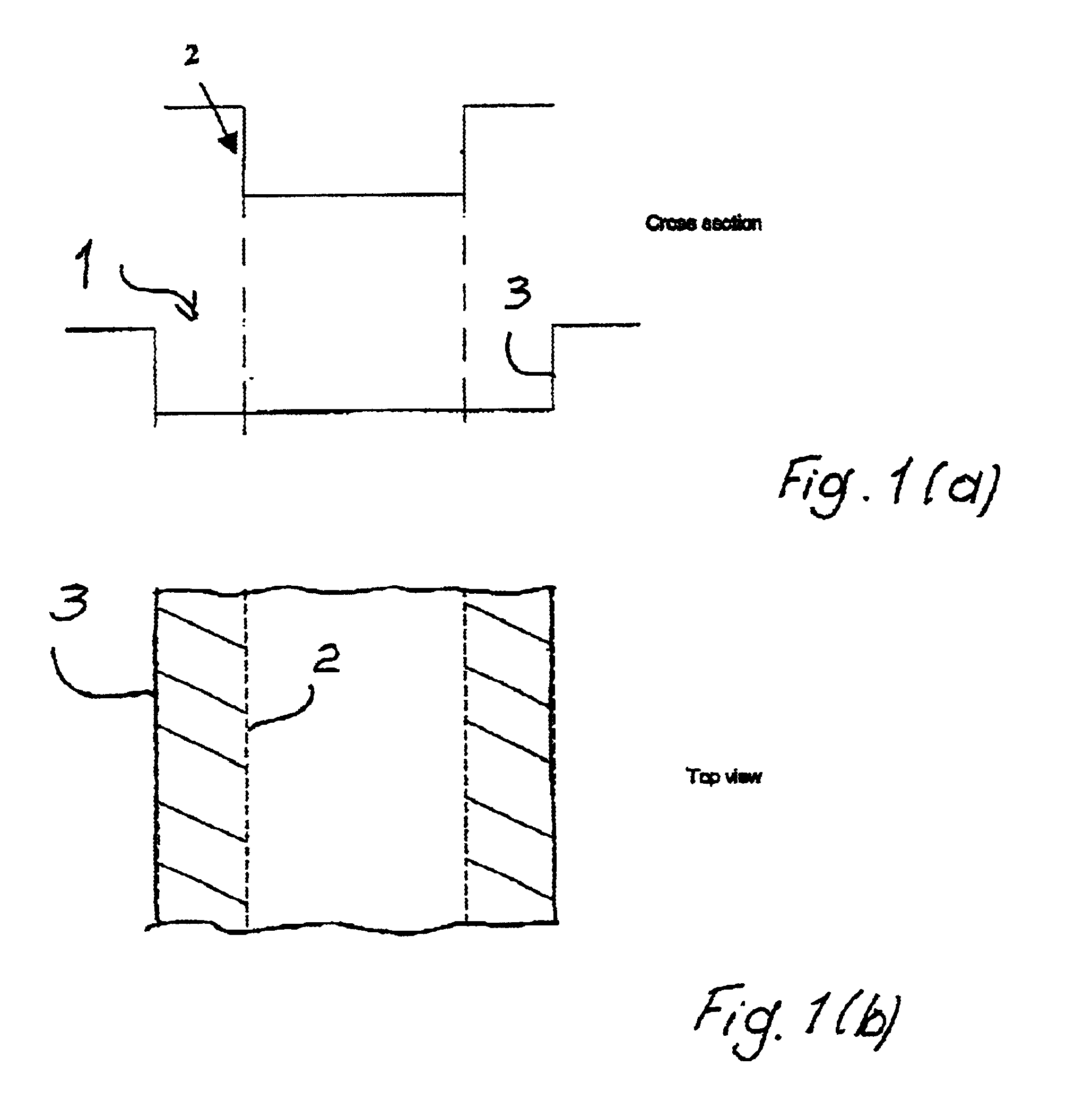
In this example a wafer is machined using a dual headed arrangement whereby the first head, Head 1 utilises a pulsed green laser source of average power larger than 6 Watts, while Head 2 utilises a pulsed 266 nm UV laser source of average power larger than 1.5 Watts. Reference is made to FIGS. 1(a) and 1(b).

The wafer is first machined by Head 1. Although the green laser is effective at achieving material removal, the overall quality of the cut edge is lower than that achievable with a UV laser system. The quality of the interior cut section and the quality of the top surface are inferior to that obtainable with UV. After the green laser of Head 1 has removed the bulk of material to form the profile 2, the UV laser of Head 2 is then used to remove material from inside and from the edges of the trench to provide the profile 3.

example 2

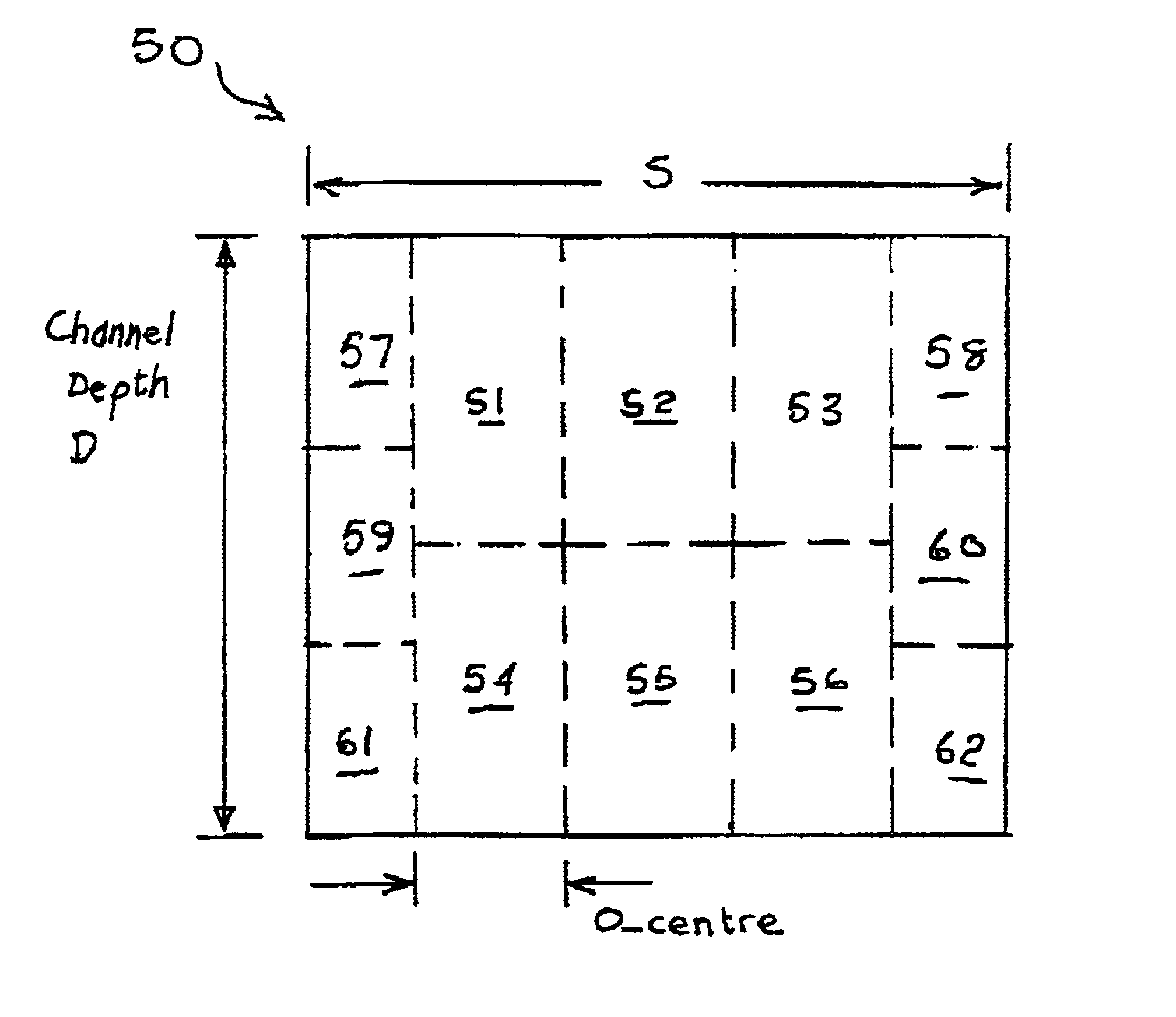
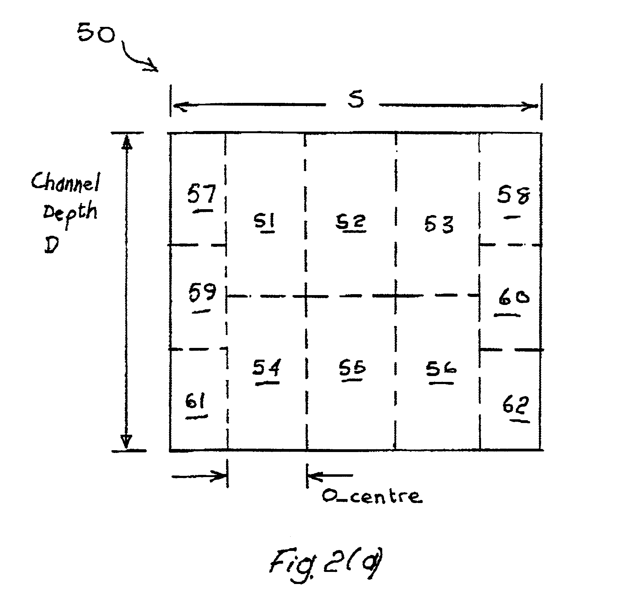
Machining a Deep Trench (FIG. 2)

Referring to FIG. 2(a) green and UV laser beams as described above for Example 1 are used to machine a deep trench 50 having a width S and a depth D.

In a first stage, a first scan of the green laser machines a rough sub-trench 51. Subsequent laterally offset scans of this laser beam machine sub-trenches 52 and 53. The lateral offset parameter is denoted “Ocenter”.

In a second stage the green laser is used to machine in succession sub-trenches 54, 55, and 56 to achieve close to dull depth D (albeit with a rough finish).

The UV laser is then used to extend laterally the trench formed by the combined sub-trenches 51 to 56. In more detail, in a third stage the UV laser is scanned around the top edge to machine out rectangular volumes 57 and 58 to a depth of c. D / 3. In a fourth stage the UV laser beam is scanned around in a rectangular path to remove the volumes 59 and 61 to a total depth of 2*D / 3. Finally, in a fifth stage the UV beam is used to machine vol...

example 3

Machining a 700 μm Silicon Wafer with a 30 μm Quartz or Fused Silica Over Layer

Referring to FIG. 3(a) a 700 micron wafer 140 with a silicon layer 141 of 670 microns and a 30 micron quartz or fused silica over layer 142, similar to that used in passive and active optical components, is represented graphically. A 9 W laser 145 at 532 nm is used for high speed machining of the silicon layer from the bottom side of the wafer, FIG. 3(b). Subsequently, a lower power UV laser beam 146 is used to accurately remove the quartz or fused silica layer 142 by machining from the top side of the wafer. This machining method is suited to the production of channels and also for dicing applications.

Straight wall cuts can be achieved by performing a number of laterally offset UV laser scans to cut beyond the quartz or fused silica layer and into the silicon substrate as shown in FIG. 3(c) to provide singulated die 148. Alternatively, the width of the trench S machined by the UV laser on the top side of...


PUM

PropertyMeasurementUnit
Timeaaaaaaaaaa
Frequencyaaaaaaaaaa
Dielectric polarization enthalpyaaaaaaaaaa

Abstract

A semiconductor is cut by directing a green laser beam of high power, and subsequently directing a UV beam along the cut line. The first beam performs cutting with relatively rough edges and a high material removal rate, and the second beam completes the cut at the edges for the required finish, with a lower material quantity removal.

Description

FIELD OF THE INVENTIONThe invention relates to the use of lasers in the machining of semiconductor materials or other materials having broadly similar properties. One example is machining of semiconductors for the purpose of singulating a single integrated circuit from an array of integrated circuits on a wafer. Another example is laser removal of semiconductor material for the purpose of defining apertures in the wafer or die.PRIOR ART DISCUSSIONIntegrated circuits are fabricated using wafers of semiconductor as the starting material. Multiple integrated circuits are manufactured simultaneously through multiple lithographic steps. One of the final stages in the integrated circuit manufacture is the singulation of the integrated circuit die from the wafer in which it is formed.Currently, the industry uses diamond bladed high precision mechanical saws to perform this function. Although this is the accepted technique there are problems with the use of such saws as they cause chipping,...

Claims


Application Information

Patent Timeline
IPC IPC(8): B23K26/36B23K26/00B23K26/06B23K26/40B23K101/40H01L21/304H01L21/78H01S3/00
CPCB23K26/063B23K26/0639H01L21/78B23K26/409H01L21/3043B23K26/4075B23K26/064B23K26/0622B23K26/40B23K2103/172B23K2103/50B23K26/402B23K26/38
Inventor BOYLE, ADRIAN
Owner XSIL TECH
Why Eureka
Try Eureka