
Optical coupling device and light-receiving circuit of same

a technology of optical coupling and light-receiving circuit, which is applied in the direction of gain control, photoelectric discharge tubes, instruments, etc., can solve the problems of difficult operation, unfavorable operation of i/v converting amplifier, and inability to adjust the gain of the i/v converting amplifier, so as to reduce the distortion of the pulse width

Inactive Publication Date: 2005-01-11
SHARP KK
View PDF13 Cites 23 Cited by
  • Summary
  • Abstract
  • Description
  • Claims
  • Application Information

AI Technical Summary

Benefits of technology

The present invention is about an optical coupling device that can transmit pulses quickly without distortion. The device includes a light emitting element and a light-receiving element, along with an impedance variable circuit and a current-to-voltage converting amplifier. The impedance variable circuit changes impedance based on the level of the input photoelectric current, which helps to reduce pulse width distortion and improve the transmission rate of the pulse. Additionally, the device may include two sets of impedance variable circuits and a dummy photodiode to further reduce common mode noise and improve the device's performance.

Problems solved by technology

Furthermore, there is unevenness in a gain of the I / V converting amplifier 18 caused by manufacturing unevenness of the receiving-side circuit.
The CMR characteristics indicate how difficult it is to operate by disturbance noise.
However, this causes a problem that the process becomes complicated because it requires a specialized processing device for forming the conductive film.
However, there is a problem that the CMR characteristics deteriorate, when the band of the amplifier is wide.
Therefore, since the noise current waveform includes a high-frequency component of 10 MHz or more, when the band of the amplifier is widened more than a band corresponding to the 25 Mbps, the high-frequency component is easily amplified, and thus easily causing the faulty operation due to noise.
This narrows an allowance for the manufacturing unevenness, thereby causing a problem that a photocoupler of high speed and high CMR is difficult to be manufactured with a sufficient yield.

Method used


Image

  • Optical coupling device and light-receiving circuit of same
  • Optical coupling device and light-receiving circuit of same
  • Optical coupling device and light-receiving circuit of same

Examples


Embodiment Construction

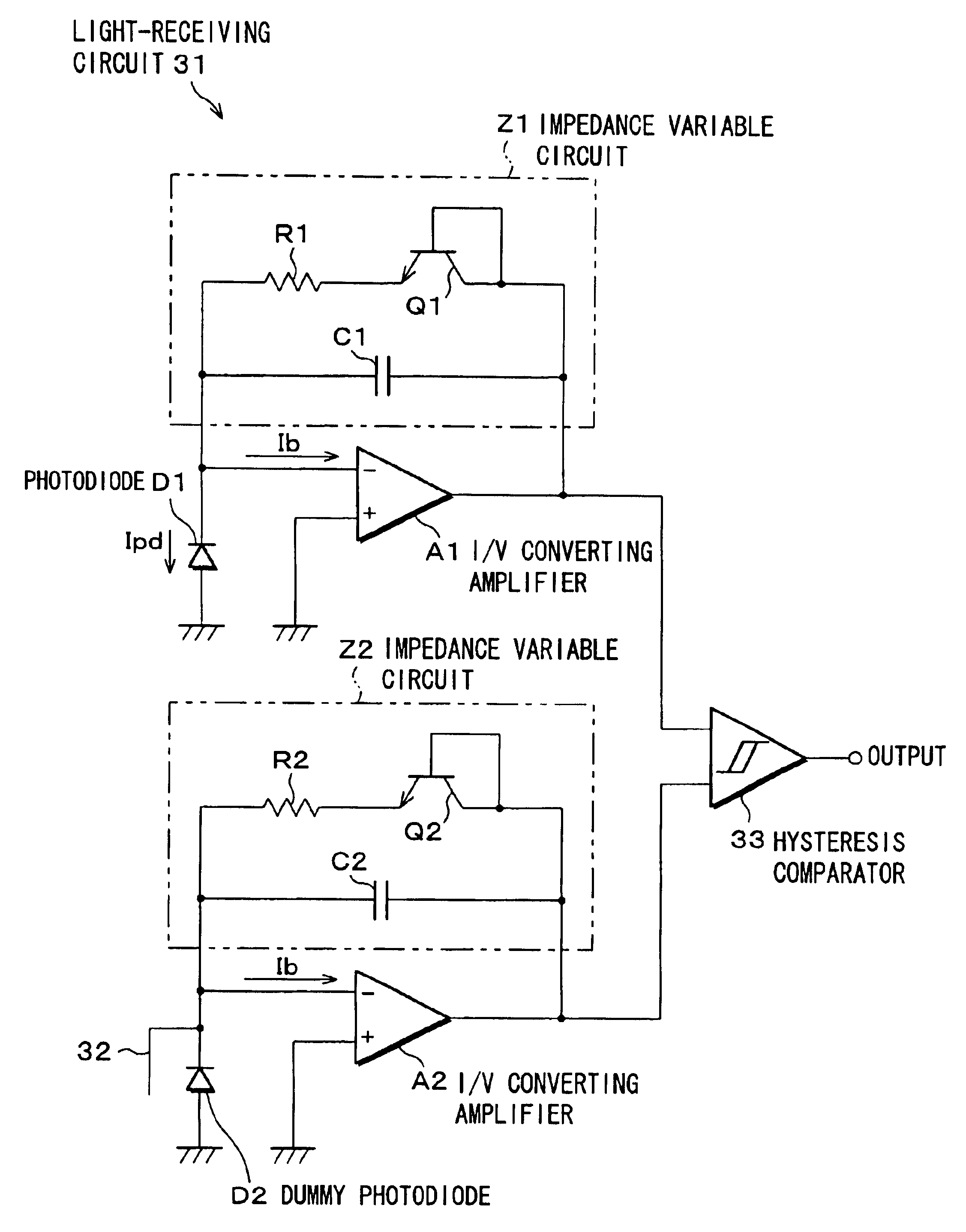
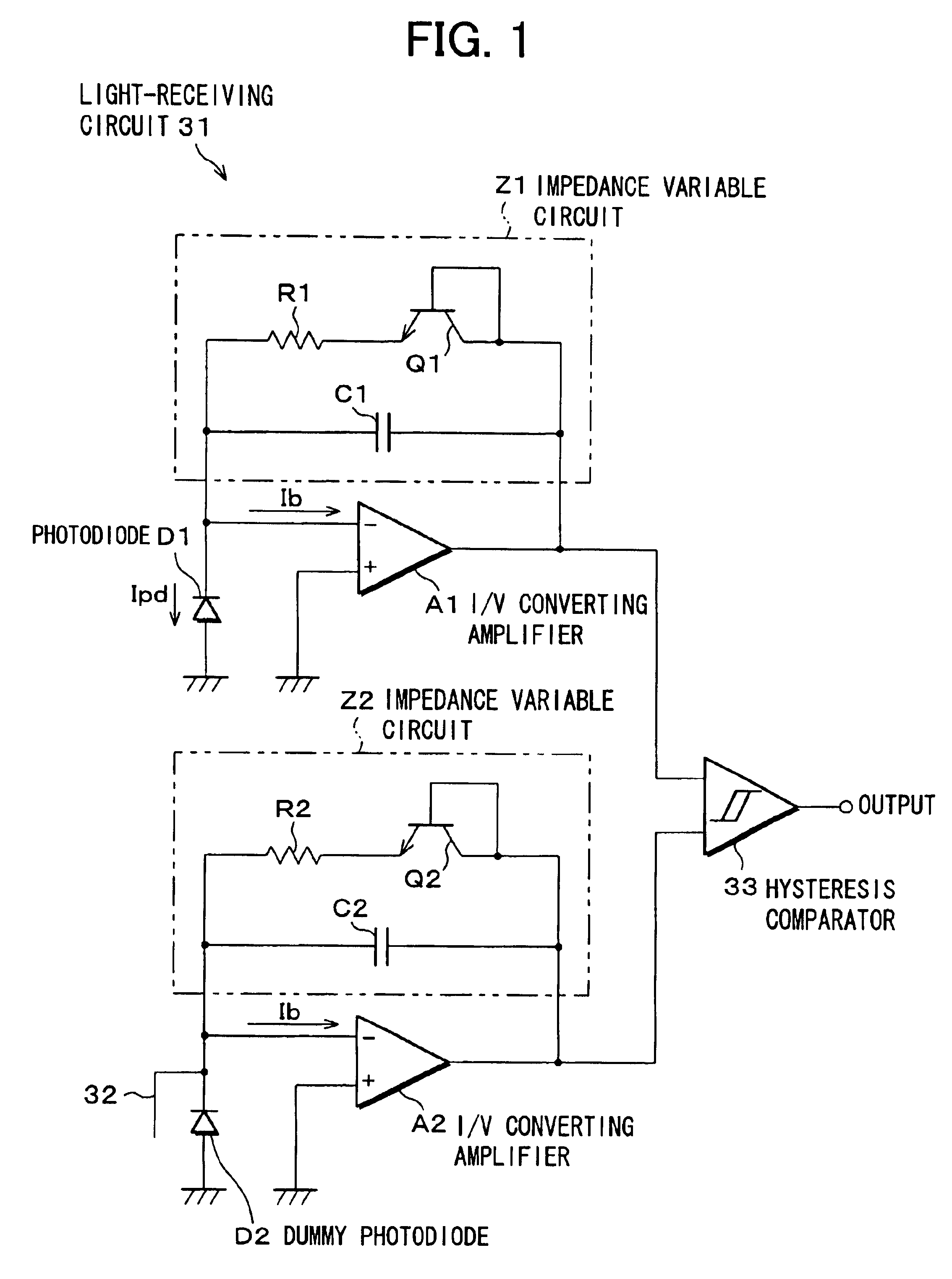
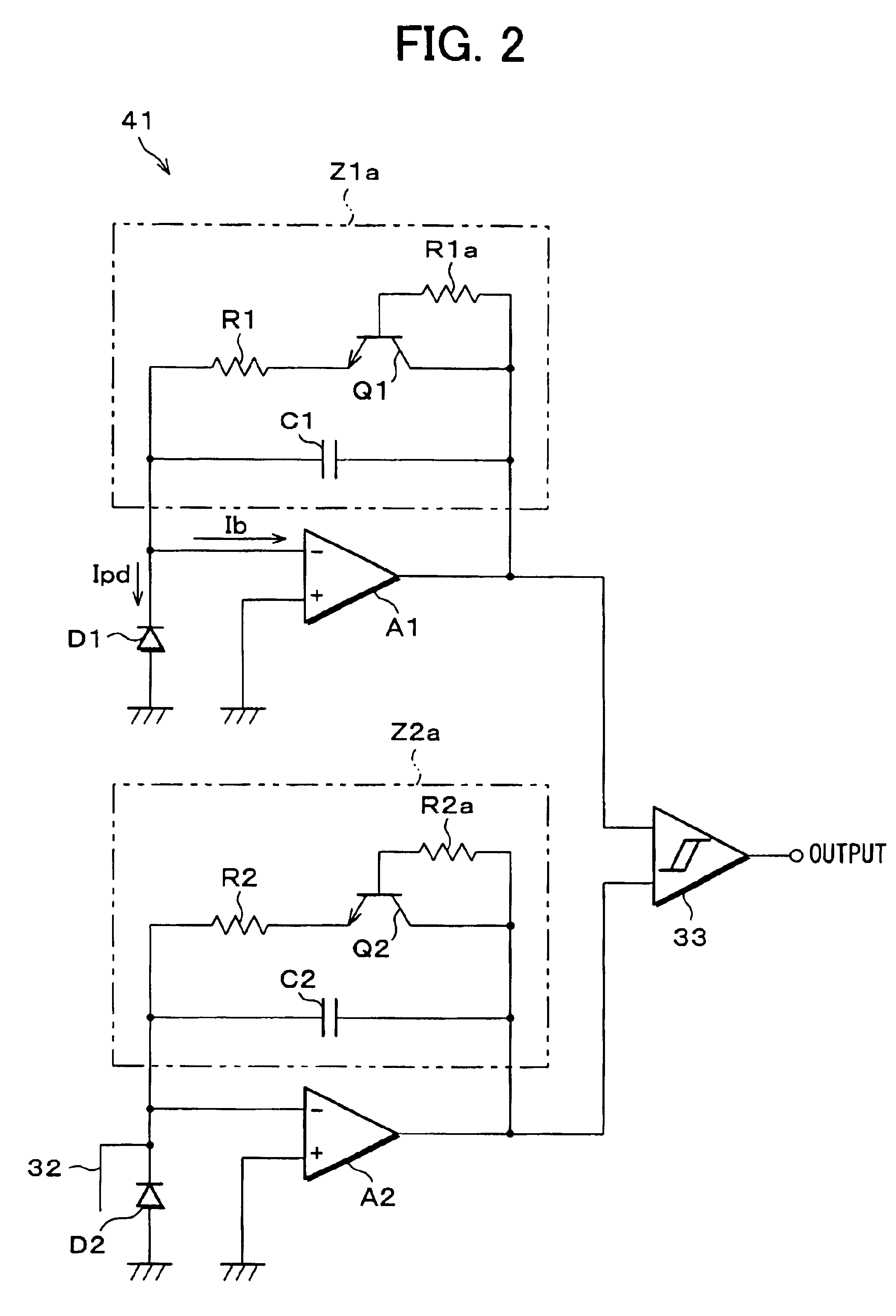
FIG. 1 is a block diagram showing an electrical arrangement of a light-receiving circuit 31 in accordance with an exemplary embodiment of the present invention. The light-receiving circuit 31 may be provided with two photodiodes D1 and D2 having identical properties in an identical shape and quantity, for example. Photodiode D1 may be used for receiving the optical signal from the light emitting element, whereas the photodiode D2 may be configured as a dummy photodiode, by its being shielded from light. The dummy photodiode D2 having its light-receiving face covered with a cathode metal wiring 32, is shielded from light where a cathode potential is applied on the cathode metal wiring 32.

Output currents from the photodiodes D1 and D2 may be converted into voltage respectively by the I / V converting amplifiers A1 and A2. The voltages may be compared with each other at a hysteresis comparator 33, which may be embodied as a differential amplifier, for example. In this way, the output fro...


PUM


Abstract

A light-receiving circuit of an optical coupling device may include a dummy photodiode arranged in a vicinity of a photodiode. The dummy photodiode and photodiode may convert received optical signals to photoelectric current. Amplified photoelectric current outputs from current-to-voltage converting amplifiers may be compared and subjected to waveform shaping by a hysterisis comparator for improving a common mode rejection ratio. Negative feedback paths and / or circuits of the converting amplifiers may include impedance variable circuits. The impedance variable circuits may reduce impedance based on the level of the input photoelectric current.

Description

BACKGROUND OF THE INVENTION1. Field of the InventionThe present invention relates, in general to an optical coupling device and a light-receiving circuit of the same.2. Description of the Related ArtFIG. 6 is a cross-sectional view of an arrangement for a conventional photocoupler 1. The photocoupler 1 converts an electric signal, which is inputted from a terminal 2 on a primary side, into an optical signal by a light emitting integrated circuit 3 on the primary side, converts the optical signal back into an electric signal by a light-receiving integrated circuit 4 on a secondary side, and outputs the electric signal from a terminal 5 on the secondary side. This electrically isolates a circuit on the primary side from a circuit on the secondary side, thereby realizing sending and receiving of a signal while the devices are electrically insulated from each other. A light emitting element, such as a light emitting diode, on the light emitting integrated circuit 3 and a light-receiving...

Claims


Application Information

Patent Timeline
Patent Type & Authority Patents(United States)
IPC IPC(8): H04B10/152H04B10/158H01L31/10H01L31/12
CPCH04B10/66H01L2224/48091H01L2224/48247H01L2924/3011H01L2924/3025H01L2924/00014H01L2924/00H01L2924/181H01L2924/00012
Inventor SHIMIZU, TAKAYUKI
Owner SHARP KK
Learn More