Flash memory cell and the method of making separate sidewall oxidation

a technology of flash memory and sidewall oxidation, which is applied in the direction of digital storage, semiconductor devices, instruments, etc., to achieve the effect of thin sidewall oxide and optimized sidewall insulating layer thickness

Inactive Publication Date: 2005-01-11
INFINEON TECH AG
View PDF19 Cites 23 Cited by
  • Summary
  • Abstract
  • Description
  • Claims
  • Application Information

AI Technical Summary

Benefits of technology

The invention overcomes the problems of the prior art by optimizing sidewall oxidation processes and temperature for logic and linear transistors and for the flash memory transistor by using a dual hard mask (HM) approach. The logic and linear transistors are formed with one hard mask and the flash memory transistors are formed with another hard mask. A typical hard mask is formed from a chemical vapor deposited (CVD) TEOS (tetraethyl orthosilicade) oxide. While the additional TEOS hard mask adds several steps to the overall process, it avoids the expense of using an additional deep ultraviolet (DUV) mask to separate polysilicon for the control gate of the flash memory cells and the logic and linear transistors. The latter appears to be the only alternative for improving the existing, prior art process. More specifically, a second TEOS hard mask is added after the flash memory cell is etched. This occurs after removal of the first TEOS hard mask and formation of the flash sidewall oxide.
The invention allows the manufacturer to optimize the thickness of the sidewall insulating layer on the flash stack and the logic and / or linear stack. It enables manufacture of a device that has different sidewall dielectric thicknesses on the flash transistors and the logic and / or linear transistors. This structure overcomes the defects of prior art structures that have logic and / or linear and flash transistors with the same sidewall thickness. With the invention the logic and / or linear devices have thinner sidewall oxides and thus can be more closely spaced to provide added logic and / or linear circuitry on the substrate. In addition, the memory devices have thicker sidewall insulating layers that shield the charge stored in the interpoly dielectric layer from adversely influencing the operation of the memory transistor.

Problems solved by technology

In addition, the memory devices have thicker sidewall insulating layers that shield the charge stored in the interpoly dielectric layer from adversely influencing the operation of the memory transistor.

Method used


Image

  • Flash memory cell and the method of making separate sidewall oxidation
  • Flash memory cell and the method of making separate sidewall oxidation
  • Flash memory cell and the method of making separate sidewall oxidation

Examples


Embodiment Construction

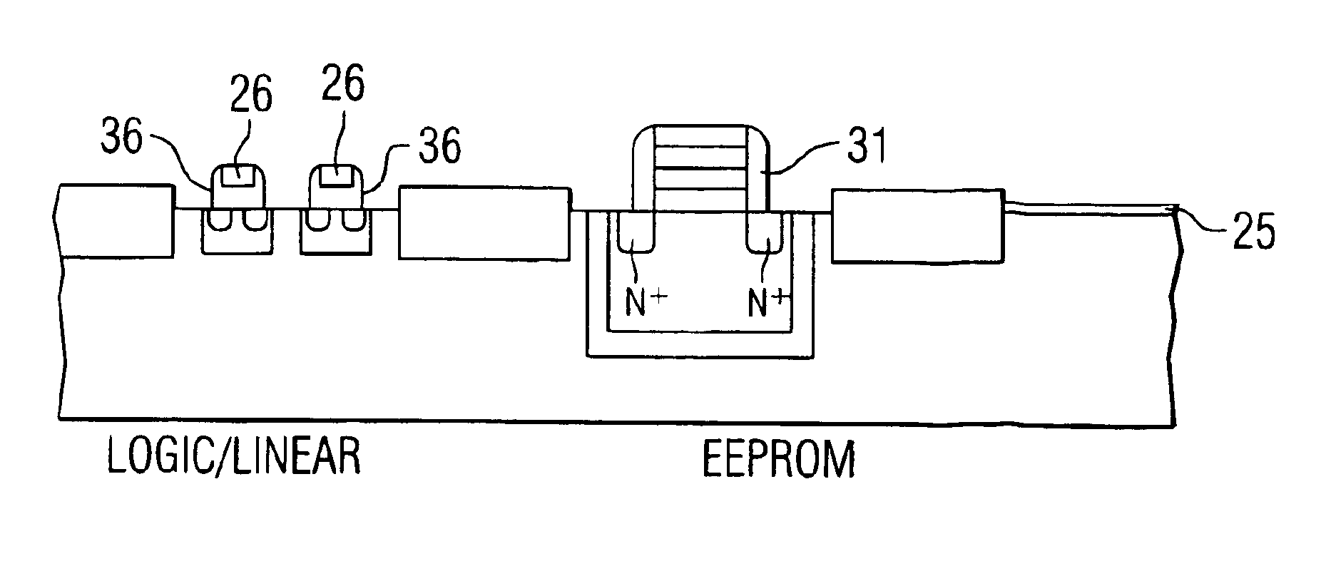
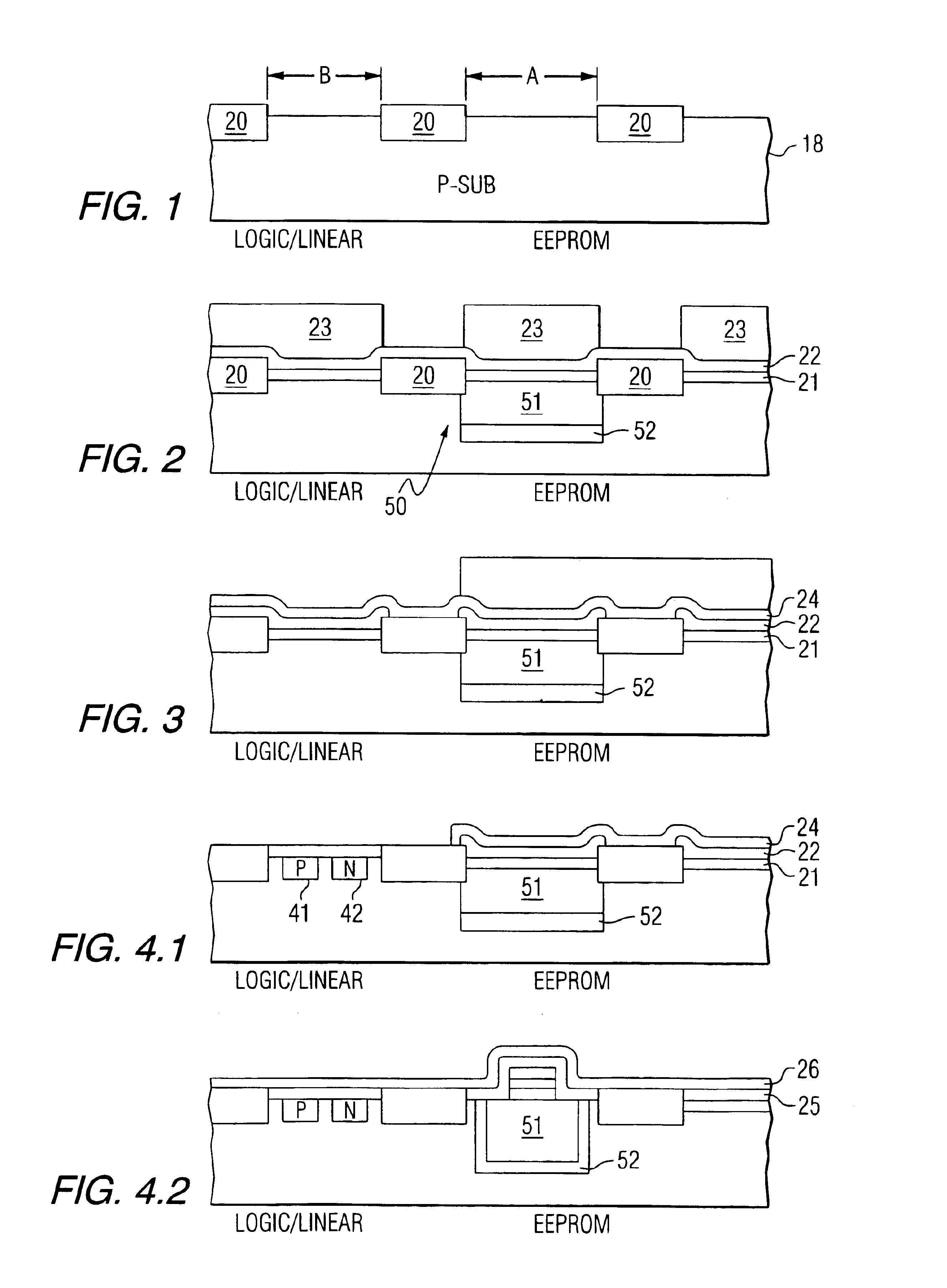
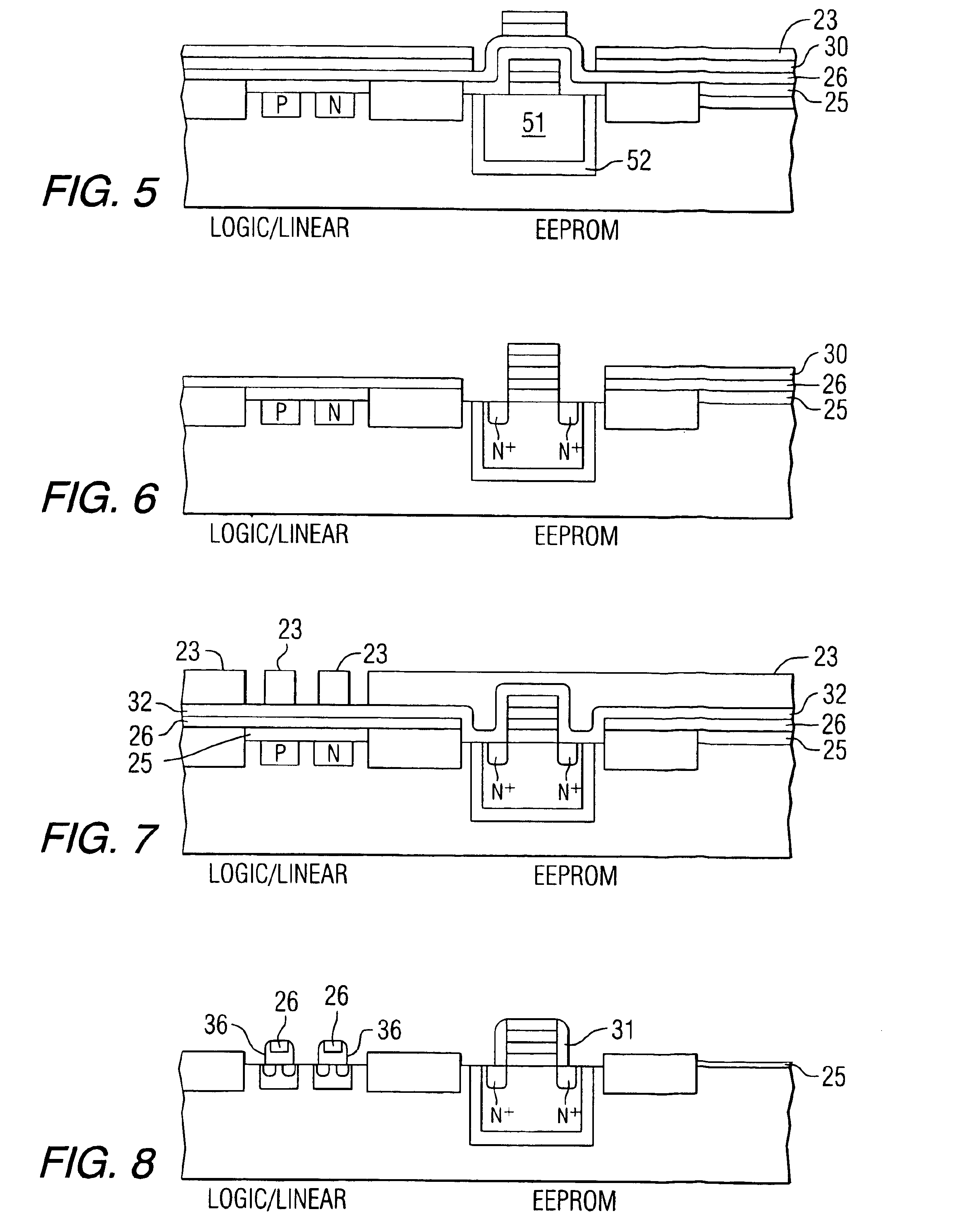
Turning to FIG. 1, a P-type substrate 18 is suitably patterned to form shallow trench isolation regions 20. The trench isolation regions 20 surround each EEPROM transistor and each pair of CMOS transistors. Those skilled in the art understand that the invention may be made on an N-type substrate where the dopings are suitable reversed. As shown in FIG. 2, the substrate is then covered with a floating gate oxide 21 followed by a layer 22 of polysilicon. Prior to deposition of the layers, a suitable portion of the substrate, such as portion A, is separately patterned and implanted to have a triple-well 50 comprising N-well 51 enclosed in a P-well 52 that resides in the P-type substrate 18. The drawing accompanying this description shows a logic CMOS pair of transistors in region B. Those regions may include transistor other than CMOS logic pairs. Those skilled in the art understand that transistor of one conductivity type may be formed in the B regions and types of transistors may be ...


PUM


Abstract

A process and product for making integrated circuits with dense logic and / or linear regions and dense memory regions is disclosed. On a common substrate, a dual hard mask process separately forms stacks of logic and / or linear transistors and EEPROM memory transistors. By using the process, the logic and / or linear and memory transistors are made with different sidewall insulating layers. The logic and / or linear transistors have relatively thin sidewall insulating layers sufficient to provide isolation from adjacent devices and conductors. The memory transistors have thicker sidewall insulating layer to prevent the charge stored in the memory device from adversely influencing the operation of the memory transistor.

Description

BACKGROUNDFlash memory cells are often fabricated on the same substrate with logic or linear transistors. In order to have an efficient manufacturing process, the transistors for the control gate in the flash memory cells and the logic and linear transistors often share the same polysilicon mask. They also share the same sidewall oxidation process and the same reactive ion etch (RIE) of the gate. While the sharing of common steps is efficient, it also presents one or more technical problems. As features sizes shrink, logic and / or linear transistors require ultra shallow source and drain junction formation to avoid short channel effect (SCE). In order to achieve such ultra shallow source and drain junction formation the thermal budget for manufacturing the device must be kept very low. As such, sidewall oxidation process must be carried out at a low temperature or be entirely dispensed with. However, flash memory cell requires significant rounding of the gate edge to reduce the high ...

Claims


Application Information

Patent Timeline
Patent Type & Authority Patents(United States)
IPC IPC(8): H01L21/70H01L21/8247H01L27/105H01L27/115H01L29/788H01L29/792
CPCH01L27/105H01L27/11546H01L27/11526H10B41/49H10B41/40
Inventor SHUM, DANNY
Owner INFINEON TECH AG
Why Eureka
Try Eureka