Active matrix liquid crystal display panel

a liquid crystal display panel and active matrix technology, applied in static indicating devices, non-linear optics, instruments, etc., can solve the problems of large difference between transmission light amount and applied voltage, remarkably deterioration of original picture image, so as to improve the degree of compensation and improve the accuracy of compensation. compensation layer, the effect of improving the degree of compensation

Inactive Publication Date: 2005-01-11
NEC LCD TECH CORP
View PDF26 Cites 76 Cited by
  • Summary
  • Abstract
  • Description
  • Claims
  • Application Information

AI Technical Summary

Benefits of technology

Where the active matrix liquid crystal display panel is constructed such that, when the voltage between the pixel electrodes and the opposing electrodes is 0, angles formed by directors of liquid crystal molecules in the liquid crystal layer with respect to a plane of the liquid crystal layer are substantially uniform, and the refractive index anisotropic axis of the optical compensation layer extends substantially in parallel to the directors, the accuracy in compensation by the optical compensation layer is improved.
Where a prod...

Problems solved by technology

In the liquid crystal display system described above, since the director moves only in a direction substantially parallel to and in the plane of the liquid crystal layer, such a problem that, as the director rises out of the plane of the liquid crystal layer as in the TN (Twisted Nematic) mode, the relationship between the transmission light amount and the applied voltage exhibits a large difference whether the liquid crystal layer is viewed from the direction of the director or from the direction of a normal to the liquid crystal layer does not occur, and a display image which looks in a similar manner from whichever direction it is viewed can be obtained over a very wide visual angle.
However, even if a special process is not performed, a significantly coloring image does not look when the liquid crystal cell is viewed from the front.
If such coloring occurs, then when image data of full colors are to be displayed, the image of the original picture is deteriorated remarkably.
As described above, with an active matrix liquid crystal display apparatus which is constructed using a transverse electric field, while a good display characteristic is obtained over a wider angle of visibility than that of the conventional TN system, there is a problem in th...

Method used


Image

  • Active matrix liquid crystal display panel
  • Active matrix liquid crystal display panel
  • Active matrix liquid crystal display panel

Examples


first embodiment

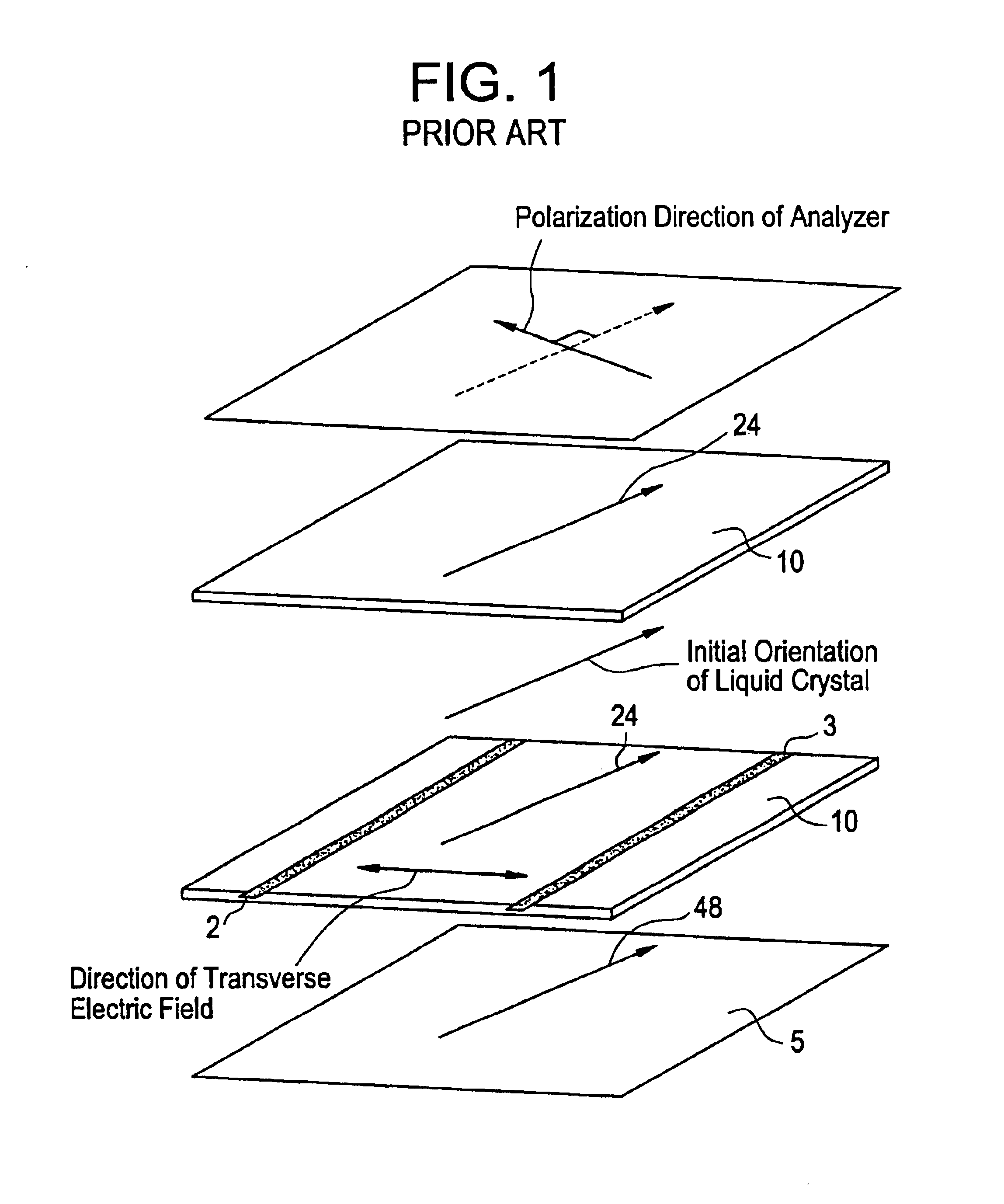
The first embodiment is described with reference to FIGS. 11(a) and 11(b). Each pixel electrode 3 which forms a pixel is connected to the source electrode of a thin film transistor which has a scanning line 16 as a gate electrode thereof, and the drain electrode of the thin film transistor is connected to a signal line 1. The pixel electrode 3 has a longitudinal direction parallel to the signal line 1 and has an opposing electrode 2 connected by an opposing electrode bus line 17.

A liquid crystal layer 4 is held between two glass substrates 10, and orientation films 23 are disposed on two substrate interfaces and are oriented uniformly in a rubbing direction 24 of FIG. 11(b) by rubbing them in the same direction.

A pair of polarizing plates 5 disposed on the outer sides of the two glass substrates 10 have polarization axes perpendicular to each other, and the polarization axis of one of the polarizing plates 5 coincides with the initial orientation direction of the liquid crystal laye...

second embodiment

FIGS. 13(a) and 13(b) are a sectional view and a plan view, respectively, showing a second embodiment of the active matrix liquid crystal display apparatus of the present invention.

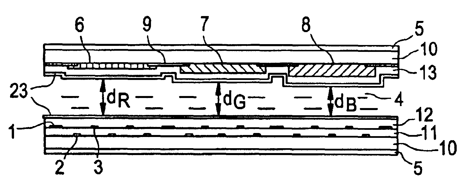
As shown in FIGS. 13(a) and 13(b), the present embodiment is quite same as the first embodiment except that the distance between a pixel electrode 3 and an opposing electrode 2 is different between a pixel 20 corresponding to green and a pixel 21 corresponding to blue and that numerical aperture adjustment portions 22 are present.

Since the distance between a pixel electrode 3 and an opposing electrode 2 is made different as seen in FIGS. 13(a) and 13(b), it can be realized by applying the same potential that the transverse electric field intensity necessary to turn the liquid crystal layer 4 is different among the different colors, which arises from a variation of the thickness of the liquid crystal layer 4. Consequently, driving is facilitated.

Further, the numerical aperture adjustment portion 22 is prov...


PUM


Abstract

An active matrix liquid crystal display panel by which a good display characteristic can be obtained without suffering from gradation reversal over a wide visibility angle range. A liquid crystal layer 4 is formed such that the thickness thereof varies in accordance with transmission wavelengths of color layers 6, 7 and 8 so that a very good display which does not exhibit any coloring in whichever direction it is viewed may be obtained.
An active matrix substrate A includes a plurality of opposing electrodes 2, a plurality of pixel electrodes 3 parallel to the opposing electrodes 2, a thin film transistor, and an orientation film 23 all formed on a glass substrate 10. A color filter substrate C includes an orientation film 56 provided on one surface of another glass substrate 10 and an optical compensation layer 35 provided on the other surface of the glass substrate 10 and formed from a plastic film. The two substrates are disposed such that the orientation films thereof oppose each other, and polarization plates 34 and 5 are disposed on the outer sides of the two substrates, and a liquid crystal layer 4 having a positive refractive index anisotropy is provided between the orientation films 23. The optical compensation layer 35 has a negative one axial refractive index anisotropy and can cancel a retardation produced in the liquid crystal layer 4 thereby to suppress white floating of a black display portion.

Description

BACKGROUND OF THE INVENTION1. Field of the InventionThis invention relates to an active matrix liquid crystal display panel of the structure wherein liquid crystal is held between transparent insulating substrates.2. Description of the Related ArtAn active matrix liquid crystal display panel (hereinafter referred to as AMLCD) wherein a thin film field effect transistor (hereinafter referred to as TFT) is used as a switching element for a pixel has a high picture quality and is utilized widely as a display device for a portable computer or a monitor for a desk top computer of the space saving type.In recent years, in order to achieve a high quality of a liquid crystal display, a display method called in-plane switching mode which makes use of a transverse electric field in order to improve the visibility angle characteristic has been proposed (for example, Asia Display '95) (Prior Art 1).According to the display method, a pixel electrode and an opposing electrode are formed in parall...

Claims


Application Information

Patent Timeline
IPC IPC(8): G02F1/1333G02F1/13G02F1/1343G02F1/1335G02F1/13363
CPCG02F1/133371G02F1/13363G02F1/133632G02F1/134363G02F2413/105G02F2413/02G02F2413/10
Inventor NISHIDA, SHINICHISUZUKI, TERUAKISUZUKI, MASAYOSHIWATANABE, MAKOTOFUJIMAKI, ERIKOHIRAI, YOSHIHIKO
Owner NEC LCD TECH CORP
Why Eureka
Try Eureka