Delay lock loop circuit useful in a synchronous system and associated methods

a synchronous memory and delay lock technology, applied in the field of delay lock loop of synchronous memory, can solve the problems of affecting the placement of the clock signal relative to the data signal, affecting the integrity of the data transfer of the memory, and affecting the propagation delay

Inactive Publication Date: 2005-01-11
ROUND ROCK RES LLC
View PDF18 Cites 69 Cited by
  • Summary
  • Abstract
  • Description
  • Claims
  • Application Information

AI Technical Summary

Benefits of technology

[0024]A method and circuitry for a delay lock loop useful in synchronizing the accessing of a memory array with a system clock is disclosed. In a preferred embodiment, the delay lock loop includes a variable delay element. The delay of the variable delay element is initially set to a minimum delay value. The system clock is then frequency divided and sent to the variable delay element, the output of which will ultimately be used to access the memory array in a synchronized manner with the system clock. The frequency divided clock and the output of the variable delay element are input to a phase detector, which creates a control signal for adjusting the delay of the variable delay element. After the signals are determined to be locked by the phase detector, an undivided clock signal version of the clock signal is sent to the variable delay element, and a frequency divided version of the output of the variable delay element is sent to the phase detector in lieu of the previous output of the variable delay element.

Problems solved by technology

Accordingly, changes in the multiplexer's operating temperature or voltage might affect its propagation delay, and likewise might adversely impact the placement of the clock signal relative to the data signal.
Accordingly, the memory's data transfer integrity can be compromised.
However, even with a frequency divider, a problem can also occur if the loop locks with the delay of variable delay 98 near the maximum of its range.

Method used


Image

  • Delay lock loop circuit useful in a synchronous system and associated methods
  • Delay lock loop circuit useful in a synchronous system and associated methods
  • Delay lock loop circuit useful in a synchronous system and associated methods

Examples


Embodiment Construction

acterizing operation of the phase detector and charge pump of FIG. 14 when the phase of the variable signal at the phase detector lags that of the reference clock input.

[0044]FIG. 17 is a schematic diagram of an exemplary charge pump.

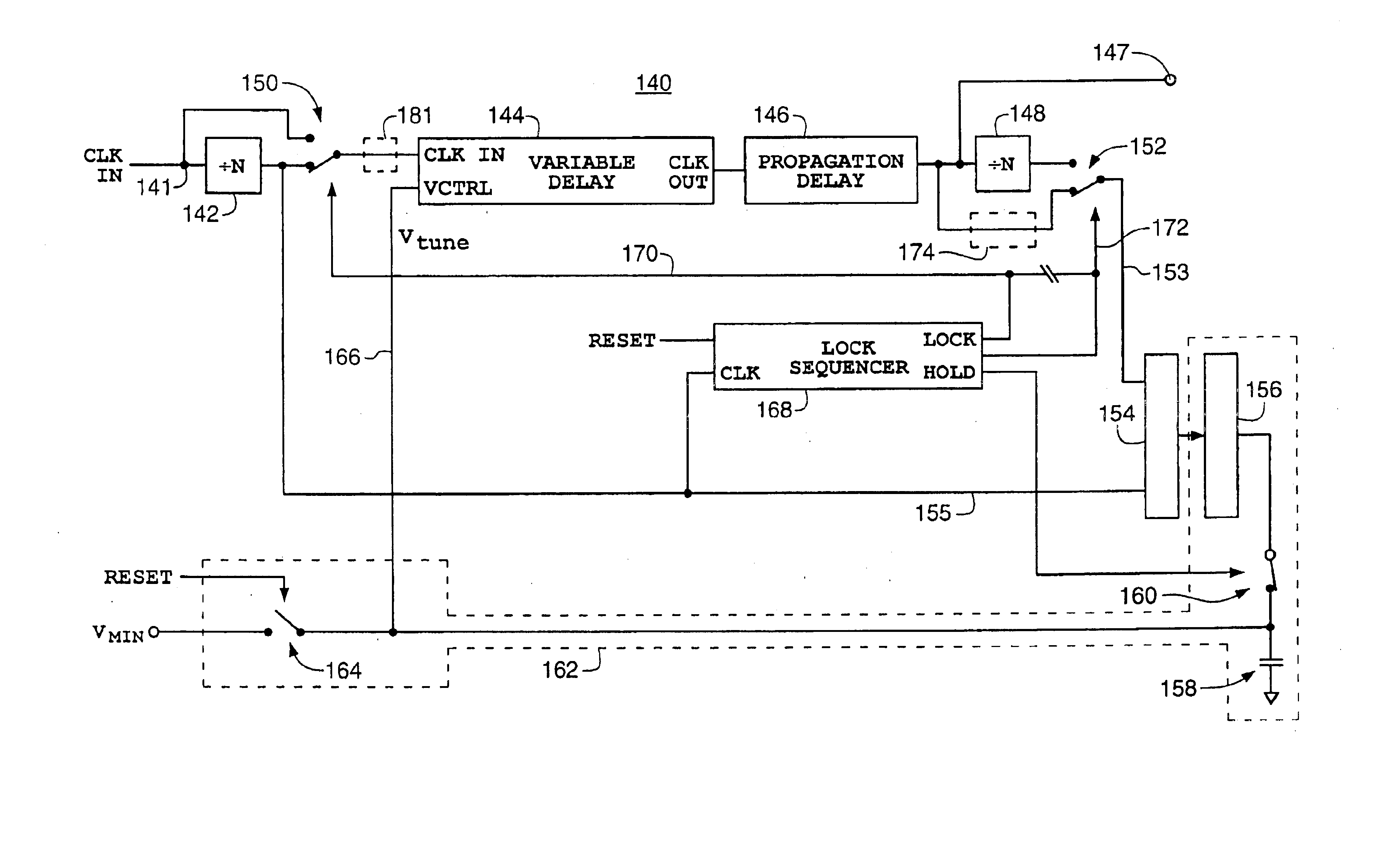
[0045]FIG. 18 is a schematic diagram of an exemplary lock sequencer for initializing a delay lock loop pursuant to an exemplary embodiment of the present invention.

[0046]FIG. 19 is a schematic diagram of an exemplary voltage clamp circuit for clamping a control signal during an initialization sequence of an exemplary embodiment of the present invention.

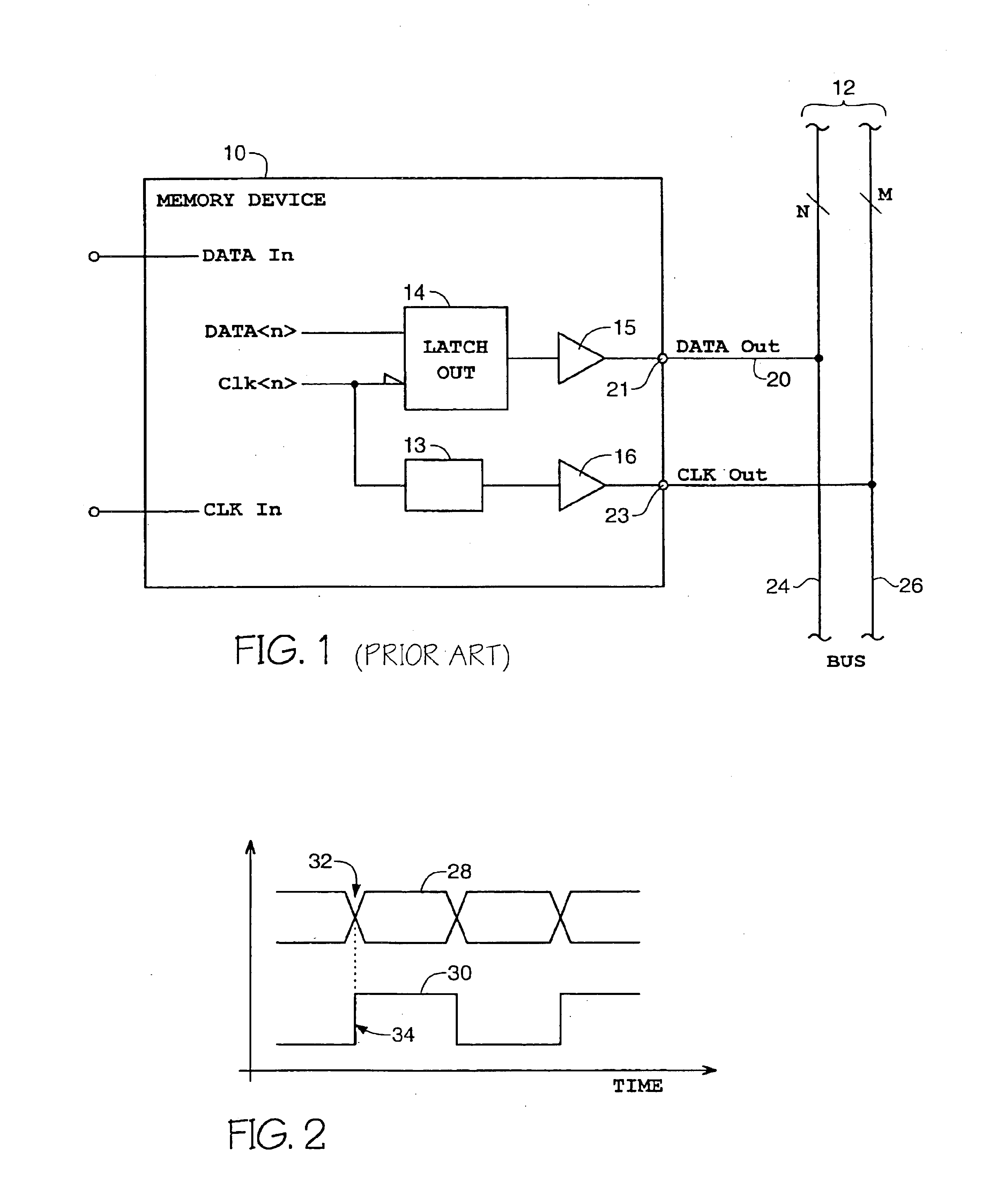
[0047]FIG. 20 is a simplified block diagram representative of a synchronous memory device, incorporating read and write data circuitry in accordance with an exemplary embodiment of the present invention.

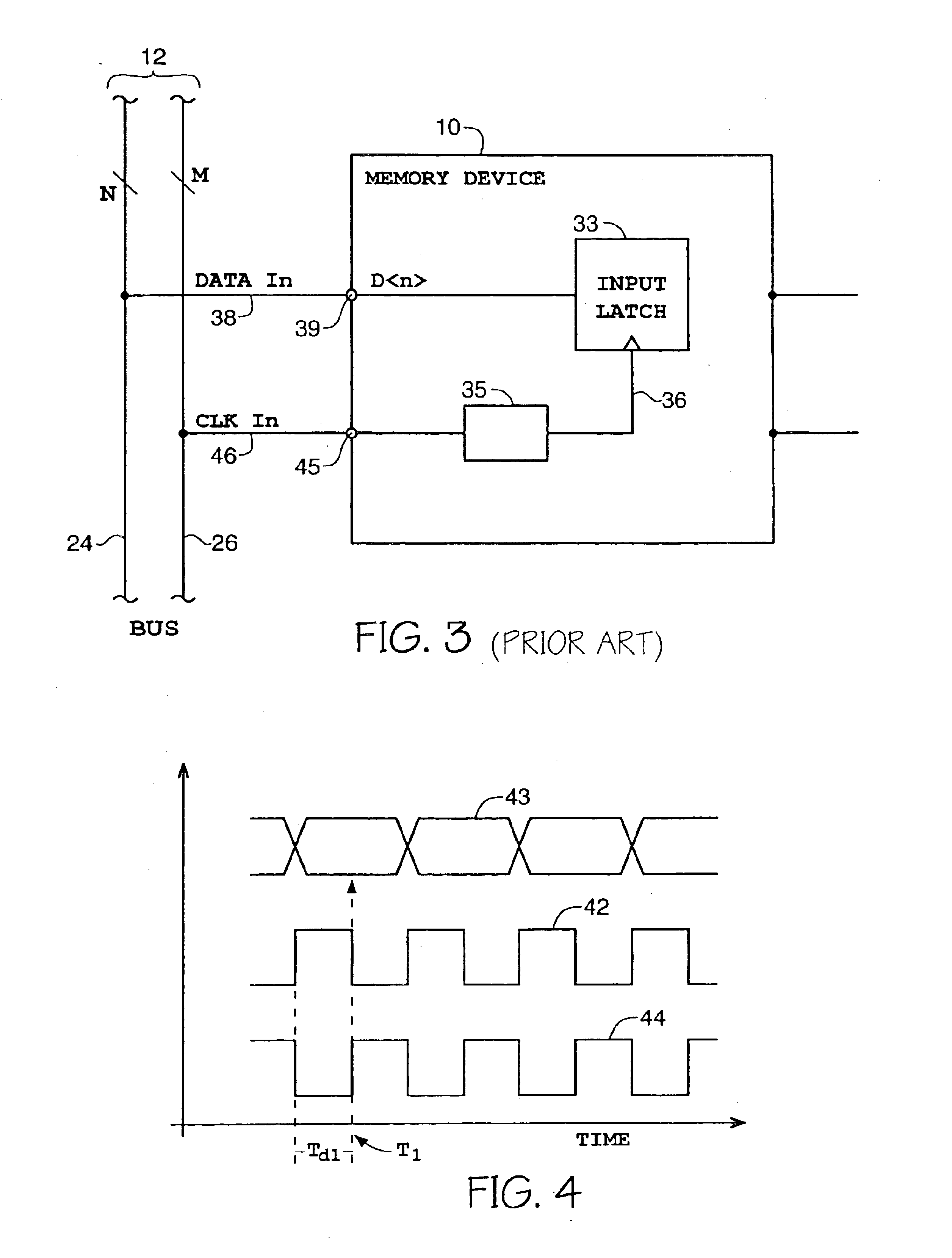
[0048]FIG. 21 is a simplified block diagram representative of a synchronous memory device, incorporating a clock initialization and synchronization circuit for a write channel of the synchronous memory dev...


PUM


Abstract

A method and circuitry for a delay lock loop useful in synchronizing the accessing of a memory array with a system clock is disclosed. In a preferred embodiment, the delay lock loop includes a variable delay element. The delay of the variable delay element is initially set to a minimum delay value. The system clock is then frequency divided and sent to the variable delay element, the output of which will ultimately be used to access the memory array in a synchronized manner with the system clock. The frequency divided clock and the output of the variable delay element are input to a phase detector, which creates a control signal for adjusting the delay of the variable delay element. After the signals are determined to be locked by the phase detector, an undivided clock signal version of the clock signal is sent to the variable delay element, and a frequency divided version of the output of the variable delay element is sent to the phase detector in lieu of the previous output of the variable delay element.

Description

[0002]This is a continuation application of, and claims priority to, U.S. application Ser. No. 10 / 230,750, filed Aug. 29, 2002, now U.S. Pat. No. 6,680,874 which is incorporated herein by reference in its entirety.BACKGROUND[0003]The present invention relates to computer systems having synchronous data transfer interfaces and also to synchronous memory devices that interface with a synchronous data bus. More particularly, the present invention relates to a delay lock loop of a synchronous memory that comprises an initialization circuit for initializing the delay lock loop to a stable and reliable operating condition.[0004]Known prior art computer systems include processors that exchange data with a variety of memory and input / output peripheral devices. Exemplary memory devices include read only memory (ROM), dynamic random access memory (DRAM), and / or static random access memory (SRAM). Exemplary input / output peripheral devices may include a keyboard, mouse, printer or video display...

Claims


Application Information

Patent Timeline
Patent Type & Authority Patents(United States)
IPC IPC(8): G11C8/00G11C8/18H03L7/089H03K23/66H03L7/081H03K23/00H03K23/54H03L7/095H03L7/085H03L7/08
CPCG11C8/18H03K23/542H03K23/66H03L7/085H03L7/0896H03L7/095H03L7/0814H03L2207/18H03L7/0816
Inventor HARRISON, RONNIE M.
Owner ROUND ROCK RES LLC
Why Eureka
Try Eureka