Semiconductor laser element and electronic device using the same

a technology of semiconductor laser and electronic device, applied in the direction of semiconductor laser, active medium material, instruments, etc., can solve the problems of difficult fabrication of laser element, dissolved emission face, difficult laser element to use as optical transmitter, etc., and achieve the effect of high speed modulation

Inactive Publication Date: 2005-01-11
SHARP KK
View PDF7 Cites 11 Cited by
  • Summary
  • Abstract
  • Description
  • Claims
  • Application Information

AI Technical Summary

Benefits of technology

Thus, the invention described herein makes possible the advantages of (1) providing a single mode oscillation laser element which operates stably at a high power for a long period and produces an almost perfectly circular emission pattern, (2) providing a high-power single mode oscillation laser element which can perform high speed modulation, and (3) providing an electronic device using one of these oscillation laser elements.

Problems solved by technology

However, in a commonly-employed semiconductor laser element, when the output level of the laser light becomes high, an emission face is dissolved.
This laser element is not suitable for use as an optical transmitter attached to a ceiling, for example.
Such a laser element is difficult to fabricate, and the production yield therefore decreases.
However, the injection of a large current into the active layer 63 may cause crystal defects, and may impede long-term, stable operation.
Therefore, the electrostatic capacitance of an entire laser element increases, and as a result, high speed modulation is not readily performed.
Such an element is not suitable for use as a light source for wireless transmission, for example.
Furthermore, since the area in which the current is injected is large, the electrostatic capacitance is large.
As a result, high speed modulation cannot be readily achieved.

Method used


Image

  • Semiconductor laser element and electronic device using the same
  • Semiconductor laser element and electronic device using the same
  • Semiconductor laser element and electronic device using the same

Examples


embodiment 1

(Embodiment 1)

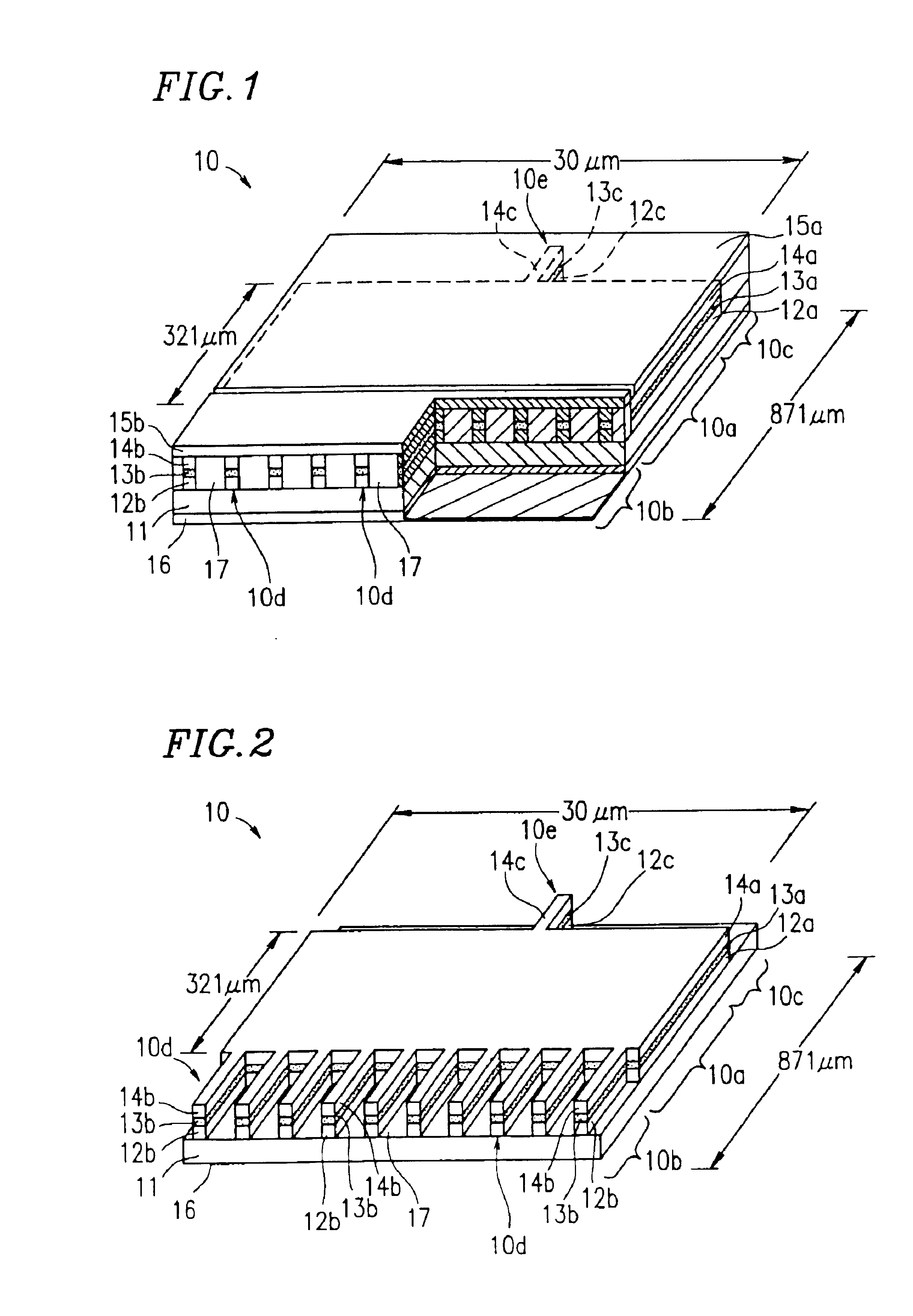
FIG. 1 is a perspective view showing a semiconductor laser device 10 according to embodiment 1 of the present invention. The semiconductor laser device 10 includes a semiconductor substrate 11 made of n-type GaAs. The semiconductor substrate 11 has a rectangular surface in which the longitudinal length is 871 μm, and the width is 30 μm. (Hereinafter, the longitudinal direction of the semiconductor substrate 11 and the direction of the width of the semiconductor substrate 11 are simply referred to as “longitudinal direction” and “width direction”, respectively.) FIG. 1 is exaggerated so that the longitudinal length of the semiconductor substrate 11 is schematically shorter than the width thereof. The entire lower surface of the semiconductor substrate 11 is covered with a negative electrode 16.

In a central region of the semiconductor substrate 11, a multimode interference (MMI) region 10a of 321 μm along the longitudinal direction is provided. On one side of the MMI reg...

embodiment 2

(Embodiment 2)

FIG. 5 is a perspective view showing a semiconductor laser element 10′ according to embodiment 2 of the present invention. (It should be noted that in the embodiments of the present invention, like reference numerals denote like elements.) The lengths of a positive electrode 15a′ for bias and a positive electrode 15b′ for modulation of the semiconductor laser element 10′ in a longitudinal direction are different from those of the positive electrode 15a for bias and the positive electrode 15b for modulation of the semiconductor laser element 10.

The fabrication method of the semiconductor laser element 10′ will not be described in detail because it is the same as that described for embodiment 1. A semiconductor laser region 10b, an MMI region 10a, and an output waveguide region 10a are integrally formed as shown in FIG. 2. In embodiment 1, as shown in FIG. 1, the positive electrode 15b for modulation (for laser emission) is formed over the semiconductor laser portions 10...

embodiment 3

(Embodiment 3)

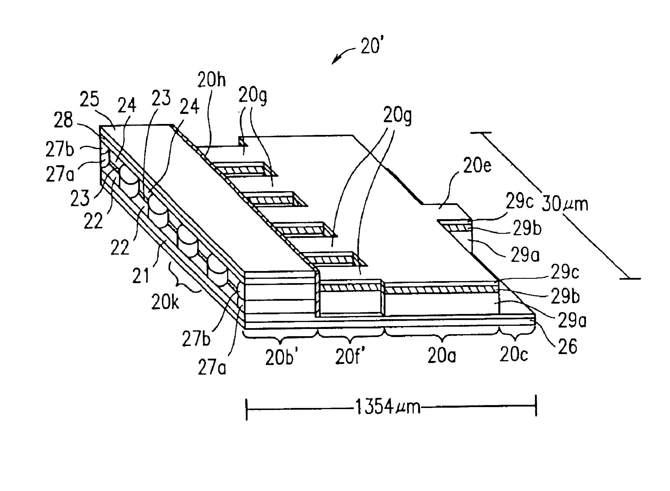
FIG. 6 is a perspective view showing a semiconductor laser device 20 according to embodiment 3 of the present invention. The semiconductor laser device 20 includes a semiconductor substrate 21 made of n-type GaAs. The semiconductor substrate 21 has a rectangular surface in which the longitudinal length is 1096 μm, and the width is 30 μm. (Hereinafter, the longitudinal direction of the semiconductor substrate 21 and the direction of the width of the semiconductor substrate 21 are simply referred to as “longitudinal direction” and “width direction”, respectively.) A negative electrode 26 is provided on the entire lower surface of the semiconductor substrate 21. FIG. 6 is exaggerated so that the longitudinal length of the semiconductor substrate 21 is schematically shorter than the width thereof.

On one side of the semiconductor substrate 21 with respect to the longitudinal direction thereof is a semiconductor laser region 20b (250 μm long in the longitudinal direction). T...


PUM


Abstract

A semiconductor laser element includes: a semiconductor laser region in which at least one laser emission portion including an active layer for emitting light is provided; a multimode interference region including a first wave-guiding layer, one end of the first wave-guiding layer being optically coupled to the active layer of the at least one laser emission portion; and an output waveguide region including a second wave-guiding layer, the second wave-guiding layer being optically coupled to another end of the first wave-guiding layer, wherein the active layer of the at least one laser emission portion, the first wave-guiding layer, and the second wave-guiding layer are integrally formed.

Description

BACKGROUND OF THE INVENTION1. Field of the InventionThe present invention relates to a high-power and high speed modulation semiconductor laser element used as a transmission light source for wireless optical communication, and to an electronic device using the same.2. Description of the Related ArtFor a semiconductor laser element used as a transmission light source for wireless optical communication, a high-power laser element which enables high speed modulation and produces a perfectly circular, uniform radiation pattern is desirable. However, in a commonly-employed semiconductor laser element, when the output level of the laser light becomes high, an emission face is dissolved. (This phenomenon is referred to as “catastrophic optical damage (COD)”.) COD occurs as described below.In the vicinity of the emission face, there is a surface level which does not contribute to the light emission. Because of this, when a current is injected into this surface level, carriers are converted...

Claims


Application Information

Patent Timeline
Patent Type & Authority Patents(United States)
IPC IPC(8): H01S5/00H01S5/026H01S5/042H01S5/062H01S5/0625H01S5/20H01S5/22H01S5/40
CPCH01S5/026H01S5/4025H01S5/0425H01S5/0625H01S5/20H01S5/0624H01S5/04256
Inventor SHIMONAKA, ATSUSHI
Owner SHARP KK
Why Eureka
Try Eureka