Carbon nanotube light emitting device, light source, and photo coupler

a carbon nanotube and light-emitting device technology, applied in the field light sources and photo couplers, can solve the problems of inability to perform on-off modulation at high speed, research and development on high-speed modulation performance of carbon nanotube light-emitting devices had not been reported at all, and achieves high speed, easy fabrication, and high speed

Active Publication Date: 2014-11-25
KEIO UNIV
View PDF19 Cites 5 Cited by
  • Summary
  • Abstract
  • Description
  • Claims
  • Application Information

AI Technical Summary

Benefits of technology

[0037]According to the present invention, the light emitting device that can be modulated at high speed can be obtained simply by forming electrodes on a metal carbon nanotube. In the case where the obtained light emitting device is applied to optical communication, the modulation performance thereof can be expected to provide ultra high-speed communication of at least about 1 to 3 Gbps. The light emitting device can be easily fabricated on various substrates such as Si substrates by integration. Accordingly, the light emitting device is applicable to a broad range of electronic and information communication fields such as optical communication using optical fibers and optical integrated circuits made by fabrication of light emitting devices on the integrated circuits.
[0038]Moreover, the present invention has a characteristic that a continuum spectrum (continuum spectrum light source) in a wide wavelength range can be obtained, which is impossible in conventional light emitting diodes and laser diodes. In the blackbody radiation by conventional filaments and the like, high-speed modulation performance is not attained, and in the present circumstances, there is no continuum spectrum light source that can be modulated at high speed. However, according to the present invention, a continuum spectrum light source that can be modulated at high speed can be implemented.
[0039]The present invention has characteristics that (a) the light emitting device that can be modulated at very high speed can easily be integrated on silicon unlike compound semiconductors, and (b) the light emitting device that can be modulated at very high speed can be fabricated at a low cost since expensive semiconductor fabrication apparatuses for use in compound semiconductors and the like are not necessary. Accordingly, the present invention is applicable not only to optical fiber communication but also to various applications which require high-speed modulation performance such as optical integrated circuits on silicon substrates, short-distance information transmission between chips and between boards, and photo couplers.

Problems solved by technology

However, research and development on high-speed modulation performance of the carbon nanotube light emitting devices had not been reported at all and the field thereof had not yet been explored.
However, in the case of light emission in the form of filaments, on-off modulation cannot be performed at high speed just as in the case of tungsten electric bulbs.
However, high speed modulation is difficult in thick carbon nanotubes, and therefore high speed modulation is not yet attempted therein.
However, in the blackbody radiation by conventional filaments and the like, high-speed modulation performance is not attained.
However, it is necessary (1) to observe a substrate with the carbon nanotube grown thereon under a microscope to find out the one carbon nanotube, or (2) to select, out of a large number of devices which were fabricated, one device accidentally formed as a single electrode.
Accordingly, yields of devices are generally poor.

Method used


Image

  • Carbon nanotube light emitting device, light source, and photo coupler
  • Carbon nanotube light emitting device, light source, and photo coupler
  • Carbon nanotube light emitting device, light source, and photo coupler

Examples


first embodiment

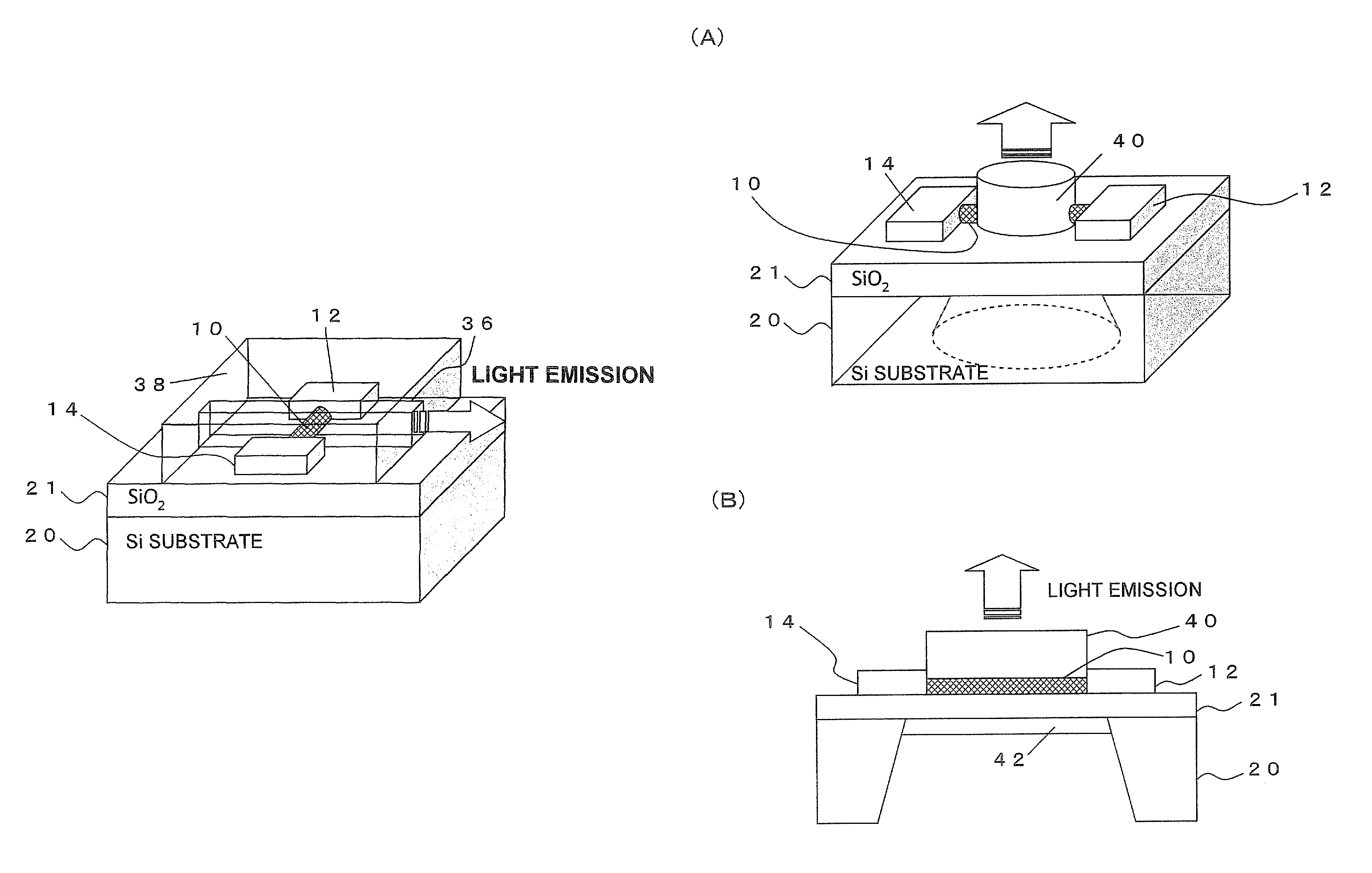
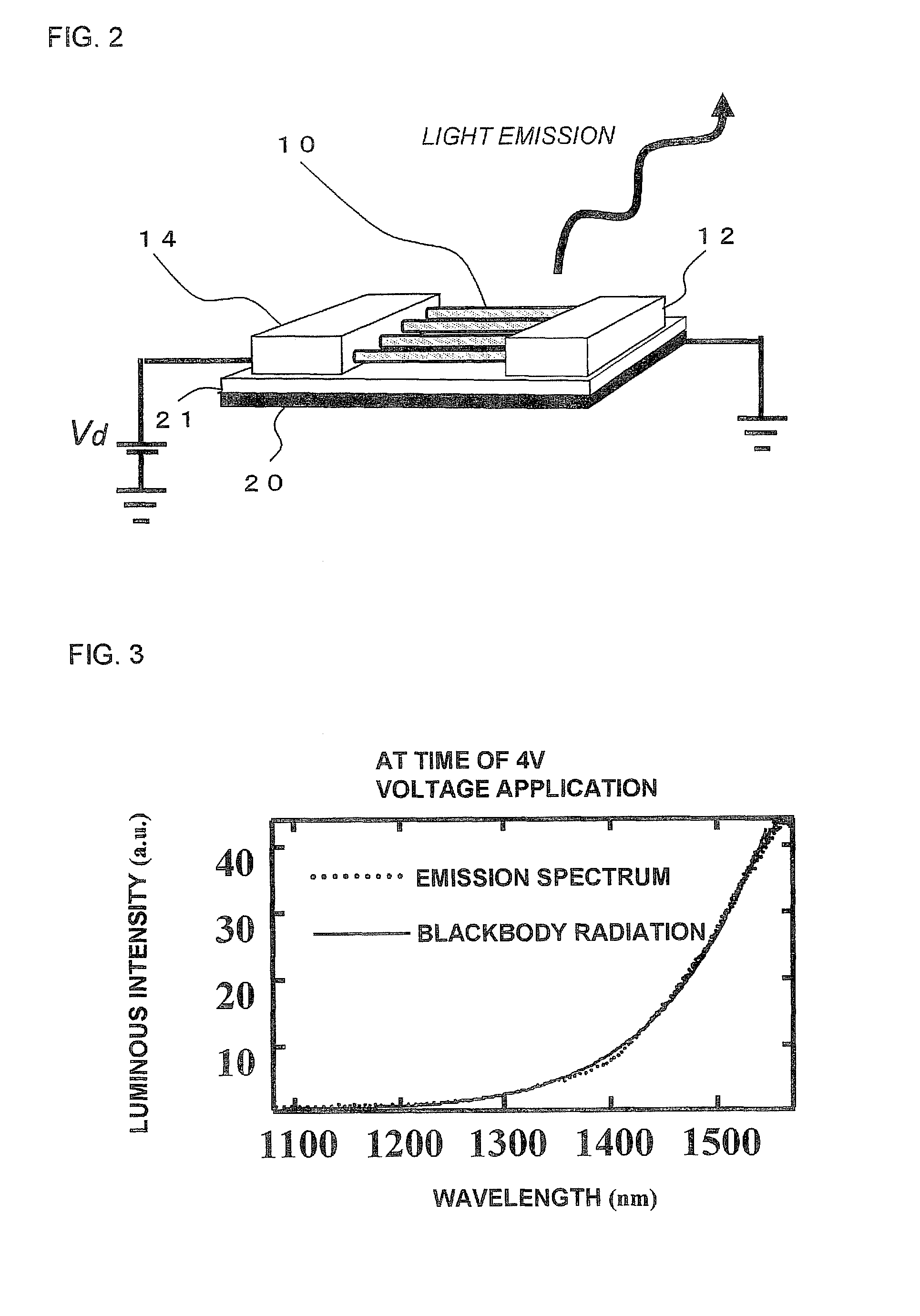
[0052]A light emitting device which is the present invention has an device configuration in which a source electrode 12 and a drain electrode 14 are formed for carbon nanotube thin films including one (one bundle of) metal carbon nanotube(s) or a plurality of metal carbon nanotubes (CNTs) 10 as shown in FIG. 2.

[0053]As a substrate 20, any kinds of substrates, such as Si, SiO2, Al2O3 and MgO substrates, may be used as long as a source-drain line is not electrically short-circuited. In the drawing, reference numeral 21 denotes a SiO2 film provided on the substrate 20.

[0054]The electrodes 12 and 14 may take any shape such as a rectangular shape. They may be formed into comb shaped electrodes to provide a larger emission area. The electrodes may be made of any materials such as metal and semiconductors as long as current can pass therethrough.

[0055]As shown in FIG. 2, the carbon nanotube 10 is disposed between the source electrode and the drain electrode. The carbon nanotubes disposed b...

second embodiment

[0061]In order to achieve long-time blackbody radiation, it is preferable to provide an insulating film 16, as seen in a light emitting device which is the present invention shown in FIG. 6, to prevent reaction with oxygen in the atmosphere. The insulating film 16 may be made of any materials such as oxide insulators including SiO2, SiN, SiON, Al2O3, MgO, HfO2, etc., and polymeric-material insulators including PMMA as long as the materials have insulation properties and can transmit light.

third embodiment

[0062]A description will now be given of a continuum spectrum light source which is the present invention adequately used as a light source incident to optical fibers.

[0063]As shown in FIG. 7, the present embodiment is configured such that a core 34 of an optical fiber 32 is pressed against a light emitting device similar to the first embodiment and is bonded thereto with adhesives such as PMMA and epoxy.

[0064]According to the present embodiment, light can efficiently be made to come incident into the core34 of the optical fiber 32.


PUM

PropertyMeasurementUnit
diameteraaaaaaaaaa
currentaaaaaaaaaa
time-aaaaaaaaaa

Abstract

A plurality of electrodes, and carbon nanotubes disposed between the electrodes, at least part of the carbon nanotubes including a metal carbon nanotube are provided. The metal carbon nanotube generates heat upon passing of current to the electrodes and emits light by blackbody radiation, so that the emitted light has a wide emission wavelength region and can be modulated at high speed. This makes it possible to implement a continuum spectrum light source that can be modulated at high speed, which is suitable for use in information communication, electrical and electronic fields.

Description

TECHNICAL FIELD[0001]The present invention relates to carbon nanotube light emitting devices, light sources and photo couplers, and more particularly relates to a carbon nanotube light emitting device capable of implementing a continuum spectrum light source that can be modulated at high speed, and a light source and a photo coupler using the carbon nanotube light emitting device, which are suitable for use in information communication, electrical and electronic fields.BACKGROUND ART[0002]Research on carbon nanotubes (CNTs) is vigorously being conducted ever since light emission by the carbon nanotubes was observed by photoluminescence measurement involving light excitation to observe light emission. In recent years, light emission by the carbon nanotubes due to current injection was observed, and as a consequence, carbon nanotubes have also come to be expected as light emitting devices. Light emitting devices using carbon nanotubes have been reported in Non-Patent Literatures 1 to ...

Claims


Application Information

Patent Timeline
Patent Type & Authority Patents(United States)
IPC IPC(8): H01L51/50H01K1/06H01L29/26B82Y10/00H01L51/00H01L51/52H01L31/12H04B10/80H01L33/04H01K3/02H01L33/00B82Y30/00H01K1/10H01L27/15B82Y20/00
CPCH01L51/0048H01L51/5296H01K3/02H01L33/04B82Y20/00B82Y30/00H04B10/80H01L51/5012H01K1/06B82Y10/00Y10S977/95H01K1/10H10K85/221H10K50/11H10K50/30
Inventor MAKI, HIDEYUKIYAMAUCHI, YOUHEI
Owner KEIO UNIV
Why Eureka
Try Eureka