
Multichip module

a multi-chip module and wiring technology, applied in the direction of instruments, non-skid devices, semiconductor/solid-state device details, etc., can solve the problems of reducing the number of terminals needed, and reducing the number of terminals

Inactive Publication Date: 2005-01-18
RENESAS ELECTRONICS CORP
View PDF8 Cites 19 Cited by
  • Summary
  • Abstract
  • Description
  • Claims
  • Application Information

AI Technical Summary

Benefits of technology

It is an object of the present invention to provide a technique for checking quality of a wiring according to which a serial test signal is used to decrease the number of terminals necessary for performing the wiring quality check.
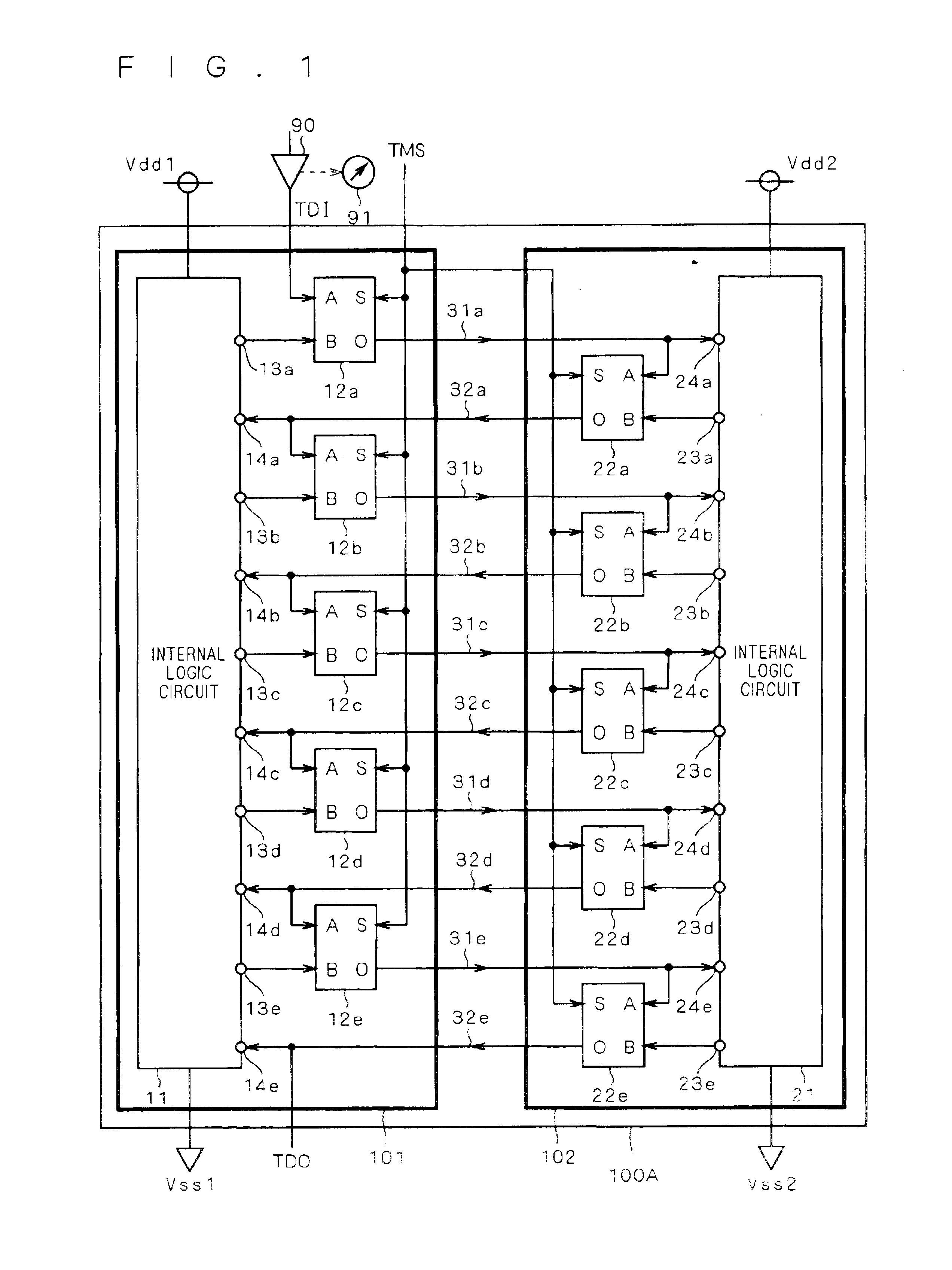
Each of the selectors of the first and second chips outputs the signal given to their second input terminals to their output terminals, to transmit and receive the signals between the first chip and the second chip. On the other hand, each of the selectors of the first and second chips can output the signal given to their first input terminals to their output terminals. In the latter case, a test signal is given to the first input terminal of the selector of the first chip to measure a detection signal from the second wiring in the first chip, thereby enabling detection of breakage failure occurring in the first wirings as well as in the second wirings. In this case, a serial signal can be used for performing the test and accordingly external connections necessary for the test signal is only two.
The output signal group is outputted from the output terminals of a plurality of output buffers of the first chip, and is transmitted via a plurality of wirings to a plurality of input buffers of the second chip. On the contrary, the signal can be transmitted from the output terminals of a plurality of output buffers of the second chip via a plurality of wirings to a plurality of input buffers of the first chip. Furthermore, a plurality of test signals can be outputted in parallel from the output terminals of the plurality of output buffers of the first chip. In this case, unless the wiring transmitting one test signal is broken, an electric potential of the third power source or the fourth power source fluctuates via a parasitic diode residing between this wiring and the third power source in response to bringing the output buffer of the second chip into an inactive condition. In an event that a short circuit is caused between the wiring transmitting one test signal and a wiring transmitting another test signal, increased current will flow between the first power source and the second power source. Therefore, it is possible to detect breakage failure or short-circuit failure in the plurality of wirings. In this case, the logic of only one test signal is different from logics of other test signals. Hence, it becomes possible to reduce the number of external connections even in a case the test signals are entered from the outside.
The selector of the first chip outputs the signal given to the first wiring group of the first chip to the plurality of first wirings. The selector of the second chip outputs the signal given to the first wiring group of the second chip to the plurality of second wirings. Accordingly, transmitting and receiving the signals between the first chip and the second chip is feasible. On the other hand, the selector of the first chip outputs the signal given to the second wiring group of the first chip to the plurality of first wirings. The selector of the second chip outputs the signal given to the second wiring group of the second chip to the plurality of second wirings. Accordingly, by comparing the output of the logic gate of the first chip with the test signal, it becomes possible to detect breakage failure occurring in the first wirings as well as in the second wirings. In this case, a serial signal can be used for performing the test and accordingly external connections necessary for the test signal is only two.
Accordingly, by letting the logic of the test signal make transition repetitively and comparing it with transition of the logic of the output of the second selector of the first chip, it becomes possible to detect breakage failure occurring in the first wirings as well as in the second wirings.

Problems solved by technology

If any defectiveness is present in the wiring, the multichip module is a defective product regardless of quality of each chip.
However, making clear the mutual relationship between function defectiveness and wiring defectiveness is not always easy.
Furthermore, in some cases, producing a signal pattern used for detecting the wiring defectiveness may be difficult.

Method used


Image

  • Multichip module
  • Multichip module
  • Multichip module

Examples


first embodiment

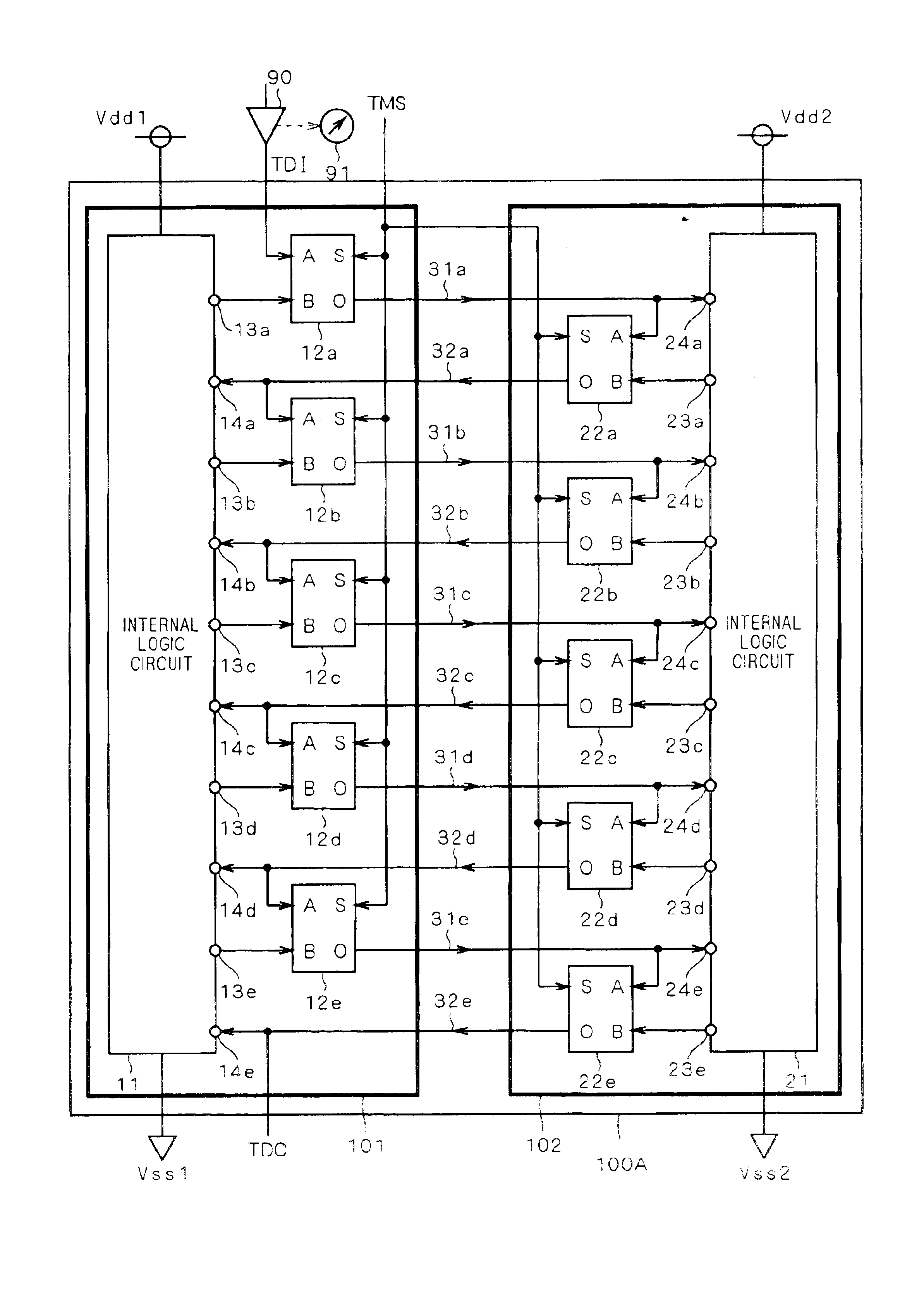
FIG. 1 is a circuit diagram showing an example of test technique in accordance with a first embodiment of the present invention. Two chips 101 and 102 are provided in a module 100A. For example, the module 100A is realized as a single package.

The module 100A has wirings 31a to 31e and 32a to 32e provided between two chips 101 and 102 for connecting these chips 101 and 102. More specifically, signals directed from the chip 101 to the chip 102 are transmitted via the wirings 31a to 31e, while signals directed from the chip 102 to the chip 101 are transmitted via the wirings 32a to 32e.

The chip 101 includes an internal logic circuit 11 and selectors 12a to 12e. The chip 102 includes an internal logic circuit 21 and selectors 22a to 22e.

The internal logic circuit 11 has signal output terminals 13a to 13e and signal input terminals 14a to 14e. The internal logic circuit 21 has signal output terminals 23a to 23e and signal input terminals 24a to 24e.

The internal logic circuit 11 is con...

second embodiment

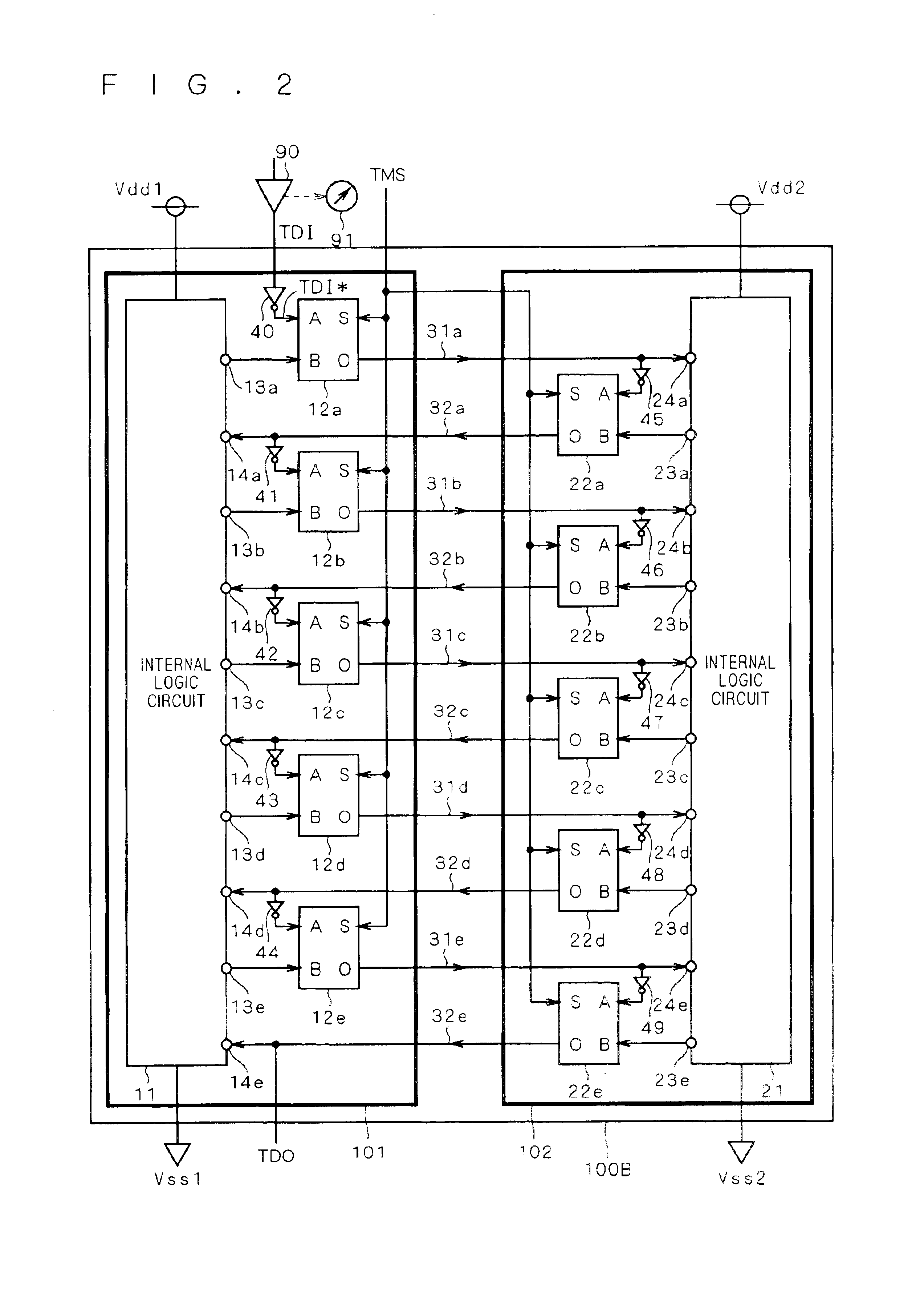
FIG. 2 is a circuit diagram showing an example of test technique in accordance with a second embodiment of the present invention. A module 100B is different from the module 100A shown in the first embodiment in that inverters 40 to 49 are additionally provided immediately in front of the first input terminals A of respective selectors 12a to 12e and 22a to 22e.

The module 100B, under the condition that the wirings 31a to 31e and 32a to 32e are normal, transmits an inverted signal TDI* of the test signal to the wirings 31a to 31e and transmits the test signal TDI to the wirings 32a to 32e when the test mode select signal TMS is activated.

According to this embodiment, like the above-described embodiment shown in FIG. 1, it is possible to detect breakage failure occurring in the wirings 31a to 31e and 32a to 32e by measuring the detection signal TDO.

Furthermore, it is possible to detect short-circuit failure occurring between the wirings 31a to 31e and the wirings 32a to 32e by detecti...

third embodiment

FIG. 3 is a circuit diagram showing an example of test technique in accordance with a third embodiment of the present invention. Two chips 101 and 102 are provided in a module 100C. For example, the module 100C is realized as a single package.

The module 100C has wirings 33a to 33d provided between two chips 101 and 102 for connecting these chips 101 and 102. Mutual transmitting and receiving signals between the chip 101 and the chip 102 is performed via the wirings 33a to 33d.

The chip 101 includes an internal logic circuit 11, a shift register group 15, a selector 17, and input / output buffers 18a to 18d. The chip 102 includes an internal logic circuit 21 and input / output buffers 28a to 28d. The number of input / output buffers 18a to 18d is identical with the number of input / output buffers 28a to 28d.

The internal logic circuit 11 is connected to a power source Vdd1 giving a high electric potential and to a power source Vss1 giving a low electric potential (e.g., a ground potential)....


PUM


Abstract

A selector has the first input terminal to which a test signal is given, the second input terminal connected to an output terminal of the first internal logic circuit, and an output terminal connected via a wiring to an input terminal of the second internal logic circuit. Another selector has an input terminal connected to the wiring, another input terminal connected to an output terminal of the second internal logic circuit, and an output terminal connected via another wiring to a signal input terminal of the second internal logic circuit. Each of the selectors selectively outputs a signal given to its first input terminal or a signal given to its second input terminal B based on a test mode signal.

Description

BACKGROUND OF THE INVENTION1. Field of the InventionThe present invention relates to a technique for checking quality of a wiring. More particularly, the present invention relates to a technique for checking quality of wirings connecting a plurality of chips which are, for example, incorporated in a single package.2. Description of the Background ArtThere is a case that a plurality of semiconductor integrated circuit chips (hereinafter, simply referred to as “chips”) are incorporated into a single package. This package is, for example, referred to as a multichip module. For example, the multichip module can realize a SIP (System In a Package).The multichip module has the wiring connecting the chips in the package. If any defectiveness is present in the wiring, the multichip module is a defective product regardless of quality of each chip.Defectiveness of the wiring is detectable through a function test applied to all of the package. However, making clear the mutual relationship betw...

Claims


Application Information

Patent Timeline
Patent Type & Authority Patents(United States)
IPC IPC(8): G01R31/28G01R31/3185H01L25/04H01L21/822H01L27/04
CPCG01R31/2818G01R31/318505G01R31/318513H01L2224/49175H01L2924/3011H01L2224/48137H01L2924/00B60C27/145
Inventor KIRITANI, MASAHIDE
Owner RENESAS ELECTRONICS CORP
Learn More