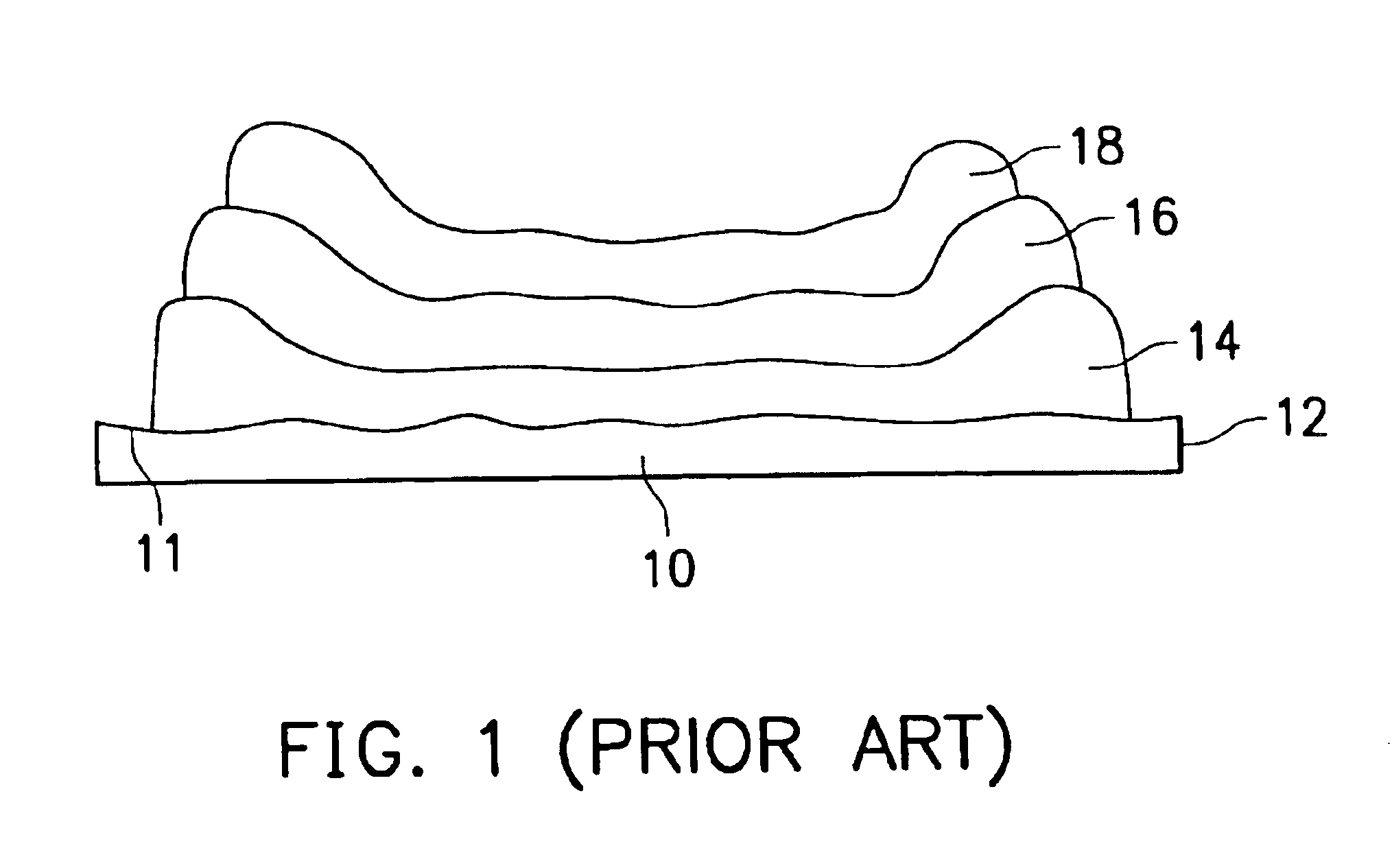
Process for improving critical dimension uniformity
a critical dimension and uniformity technology, applied in the field of process for improving critical dimension uniformity, can solve the problems of affecting yield, complex coating and etching steps, and failure to meet the requirements of the material, so as to achieve the uniformity between the wafer center and the wafer edge. the effect of enhancing the fabrication yield
- Summary
- Abstract
- Description
- Claims
- Application Information
AI Technical Summary
Benefits of technology
Problems solved by technology
Method used
Image


Examples
Embodiment Construction
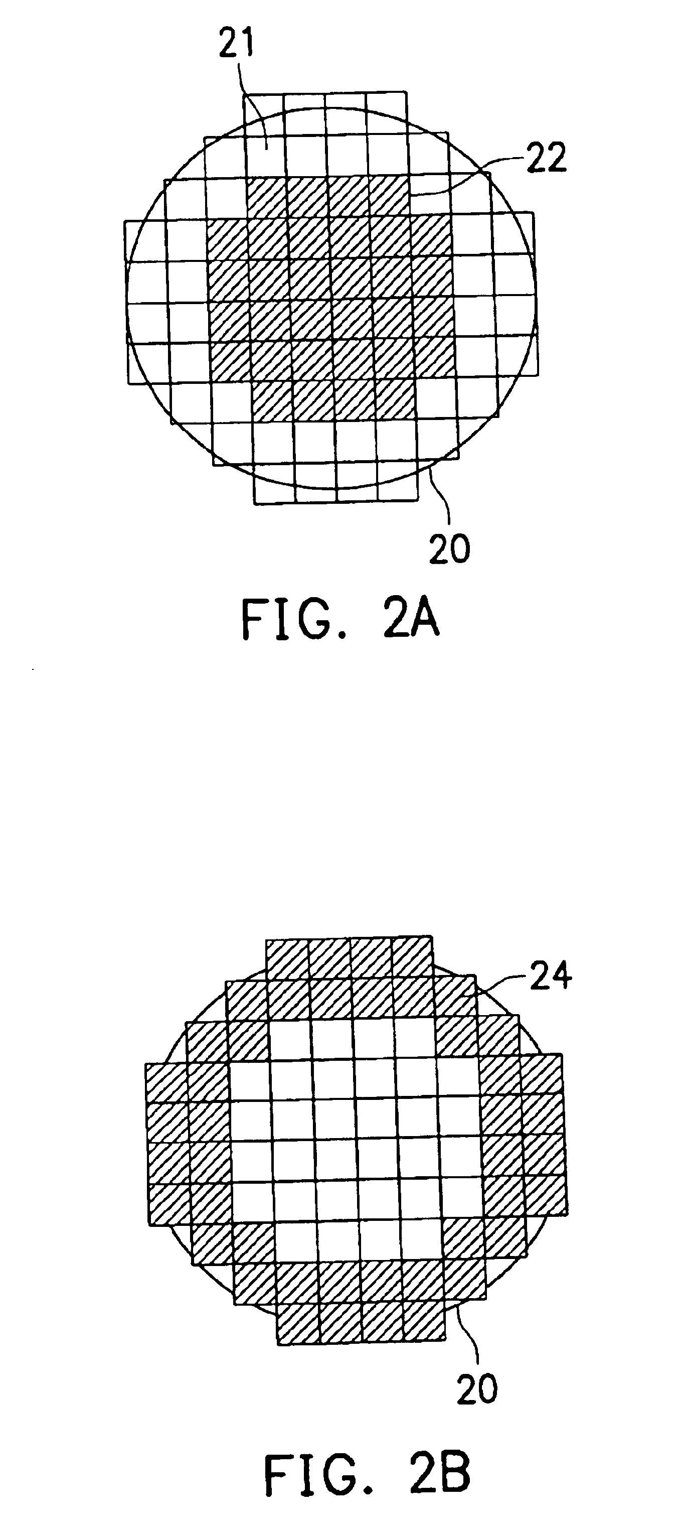
FIGS. 2A and 2B are schematic diagrams showing the first area 22 and the second area 24 defined in the embodiment of the present invention. The first area 22 and second area 24 should preferably not overlap. The region 21 is the exposure field for one time exposure in step-by-step or scan-by-scan exposure processing. Referring to FIG. 3 together with FIGS. 4B to 4J, in which FIG. 3 is the flow chart of the embodiment of the present invention and FIGS. 4B to 4J are cross-sections of the wafer corresponding to steps S300 to S380 of FIG. 3. FIG. 4A is a cross-section showing the first area aa′ and second area bb′ of a wafer according to the embodiment of the present invention.
First, as in step S300 and FIG. 4B, a coating layer 42 is formed on a wafer 20.
Then, as in step S310 and FIG. 4C, a first photoresist layer 44 is formed on the coating layer 42.
Subsequently, as in step S320 and FIG. 4D, the first photoresist layer 44 in the first area 22 is subjected to a first lithography process...
PUM
 Abstract
Description
Claims
Application Information
 - Generate Ideas
- Intellectual Property
- Life Sciences
- Materials
- Tech Scout
- Unparalleled Data Quality
- Higher Quality Content
- 60% Fewer Hallucinations
Browse by: Latest US Patents, China's latest patents, Technical Efficacy Thesaurus, Application Domain, Technology Topic, Popular Technical Reports.
© 2025 PatSnap. All rights reserved.Legal|Privacy policy|Modern Slavery Act Transparency Statement|Sitemap|About US| Contact US: help@patsnap.com