

System and method for calibrating a spatial light modulator array using shearing interferometry
a technology of spatial light modulator and interferometer, which is applied in the field of lithography, can solve the problems of increasing the cost and time of reticle manufacture, the inability to use reticles for a certain period of time before being worn out, and the routine cost of additional costs
- Summary
- Abstract
- Description
- Claims
- Application Information
AI Technical Summary
Benefits of technology
Problems solved by technology
Method used
Image

Examples
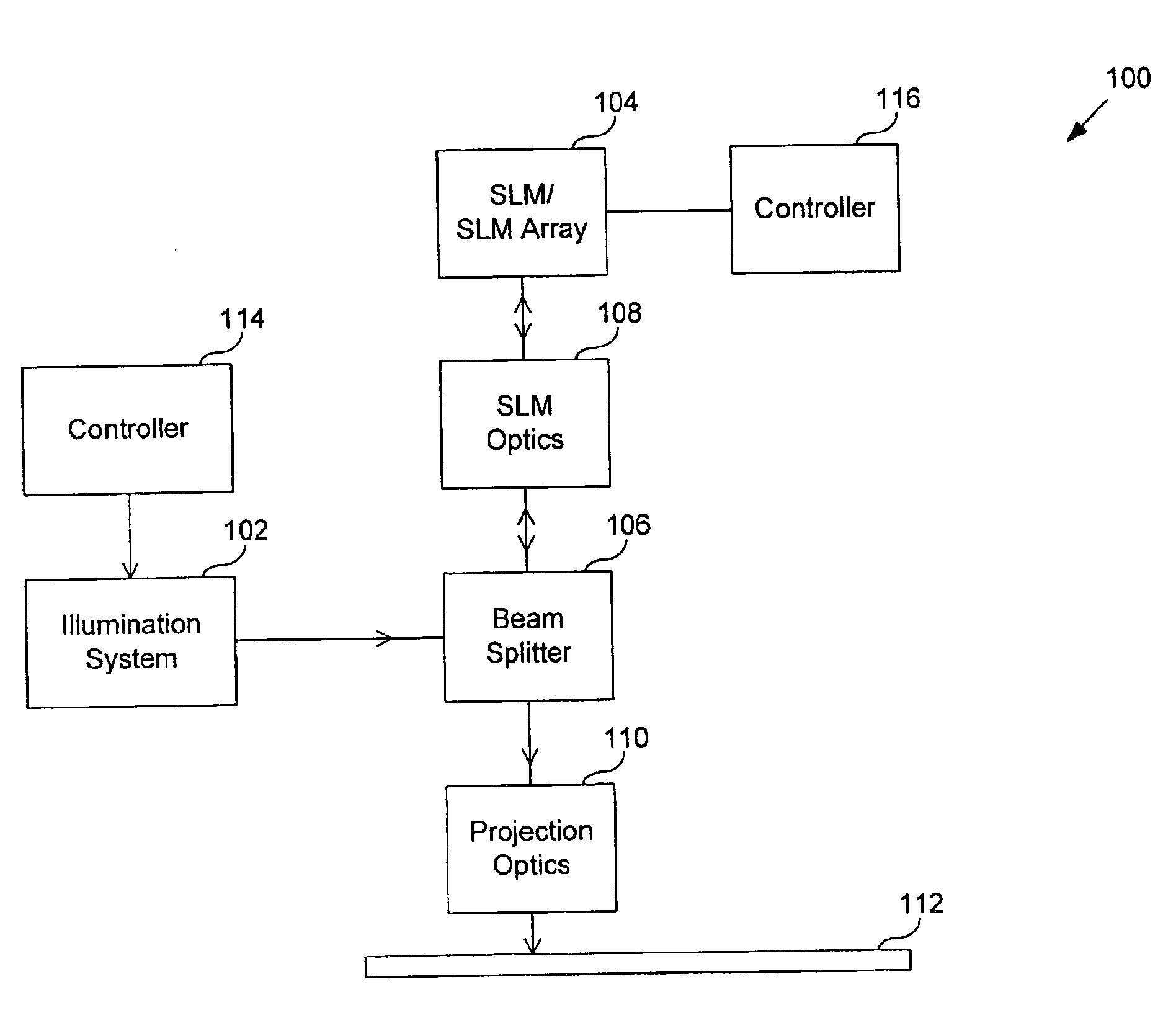
example slms
that can be used in systems 100 or 200 are manufactured by Micronic Laser Systems AB of Sweden and Fraunhofer Institute for Circuits and Systems of Germany. A grating light valve (GLV) SLM is another example of an SLM where the present invention is applicable.
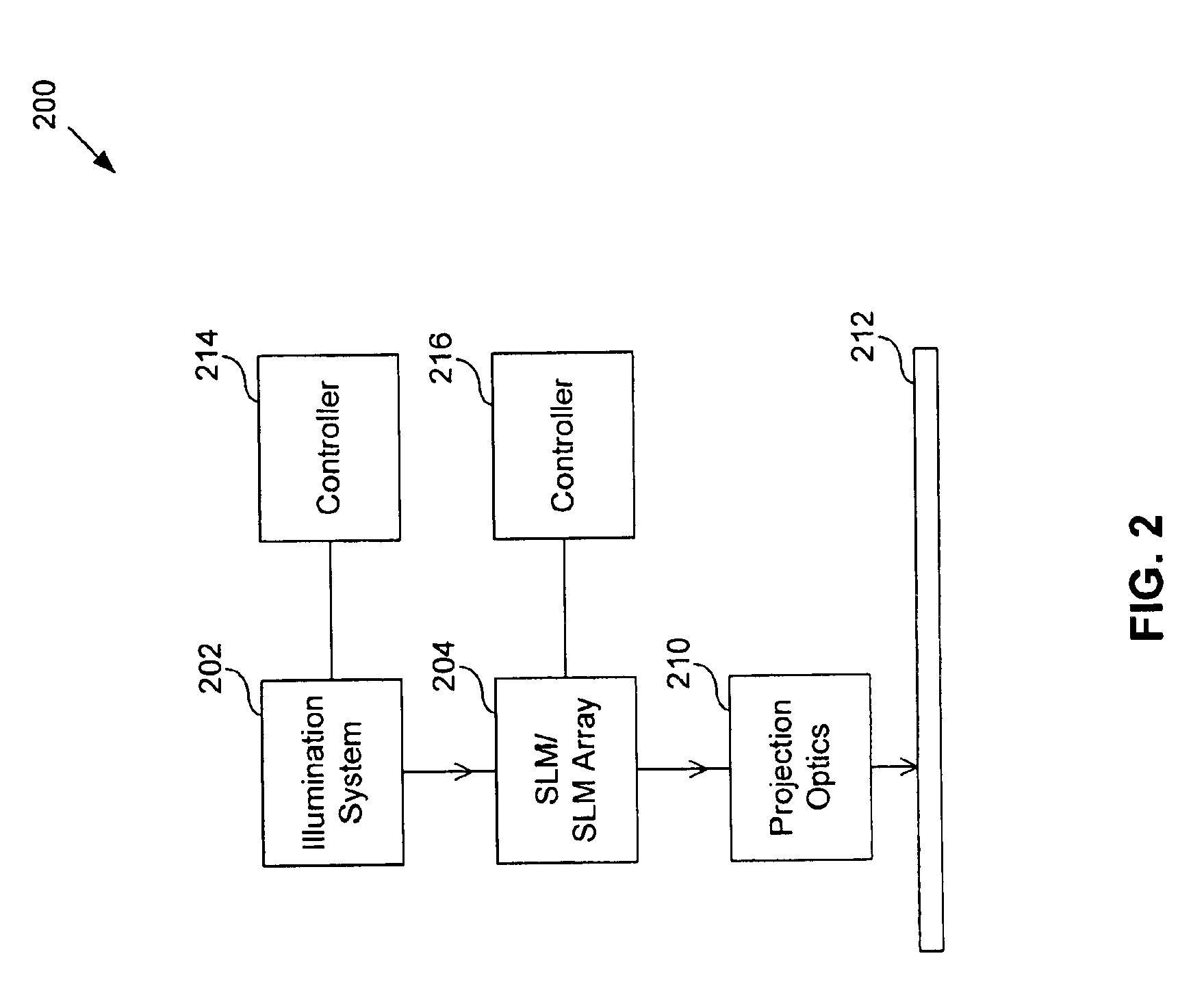
Merely for convenience, reference will be made only to system 100 below. However, all concepts discussed below can also apply to system 200, as would be known to someone skilled in the relevant arts.
FIG. 3 shows details of an active area 300 of SLM 104. Active area 300 includes an array of active devices 302 (represented by dotted patterns in the figure). Active devices 302 can be mirrors on a DMD or locations on a LCD. It is to be appreciated that active devices 302 can also be referred to as pixels, as is known in the relevant art. By adjusting the physical characteristics of active devices 302, they can be seen as being either ON or OFF (for a binary SLM) or a state in-between ON and OFF for other SLMs. Digital or analog inp...
PUM
 Abstract
Description
Claims
Application Information