Nitride semiconductor device with reduced polarization fields

a technology of nitride and semiconductor, applied in the direction of semiconductor laser, semiconductor laser structure details, lasers, etc., to achieve the effect of reducing the magnitude of piezoelectric and increasing efficiency

Inactive Publication Date: 2005-02-01
LUMILEDS
View PDF15 Cites 57 Cited by
  • Summary
  • Abstract
  • Description
  • Claims
  • Application Information

AI Technical Summary

Benefits of technology

[0014]As a result of the reduced magnitude of piezoelectric, spontaneous, or combined piezoelectric and spontaneous electric field strengths in their quantum well layers, light-emitting devices in accordance with the present invention may generate light with increased efficiency compared to prior art devices.

Problems solved by technology

This is a particularly urgent problem in GaN-based optical semiconductor devices using BN, AlN, GaN, or InN, which are compounds of nitrogen and Group III elements such as B, Al, Ga, and In and their mixed crystal semiconductors (hereinafter, called GaN-based semiconductors).

Method used


Image

  • Nitride semiconductor device with reduced polarization fields
  • Nitride semiconductor device with reduced polarization fields
  • Nitride semiconductor device with reduced polarization fields

Examples


second embodiment

[0021]FIG. 7 is a cross-sectional view of a light-emitting device according to the present invention.

third embodiment

[0022]FIG. 8 is a cross-sectional view of a light-emitting device according to the present invention.

DETAILED DESCRIPTION

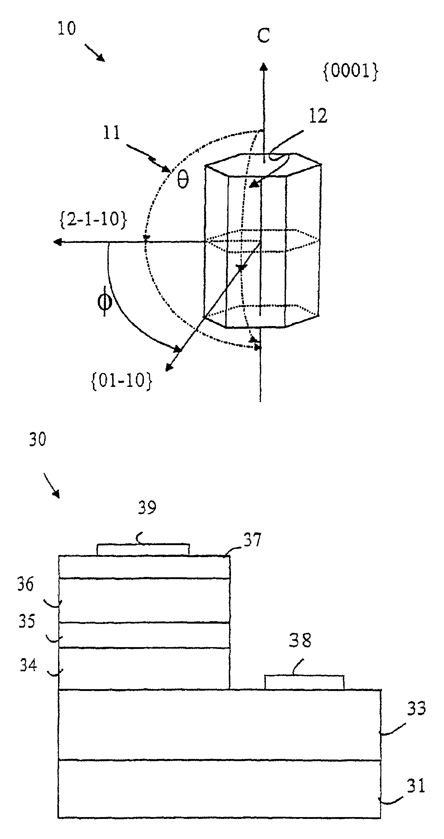
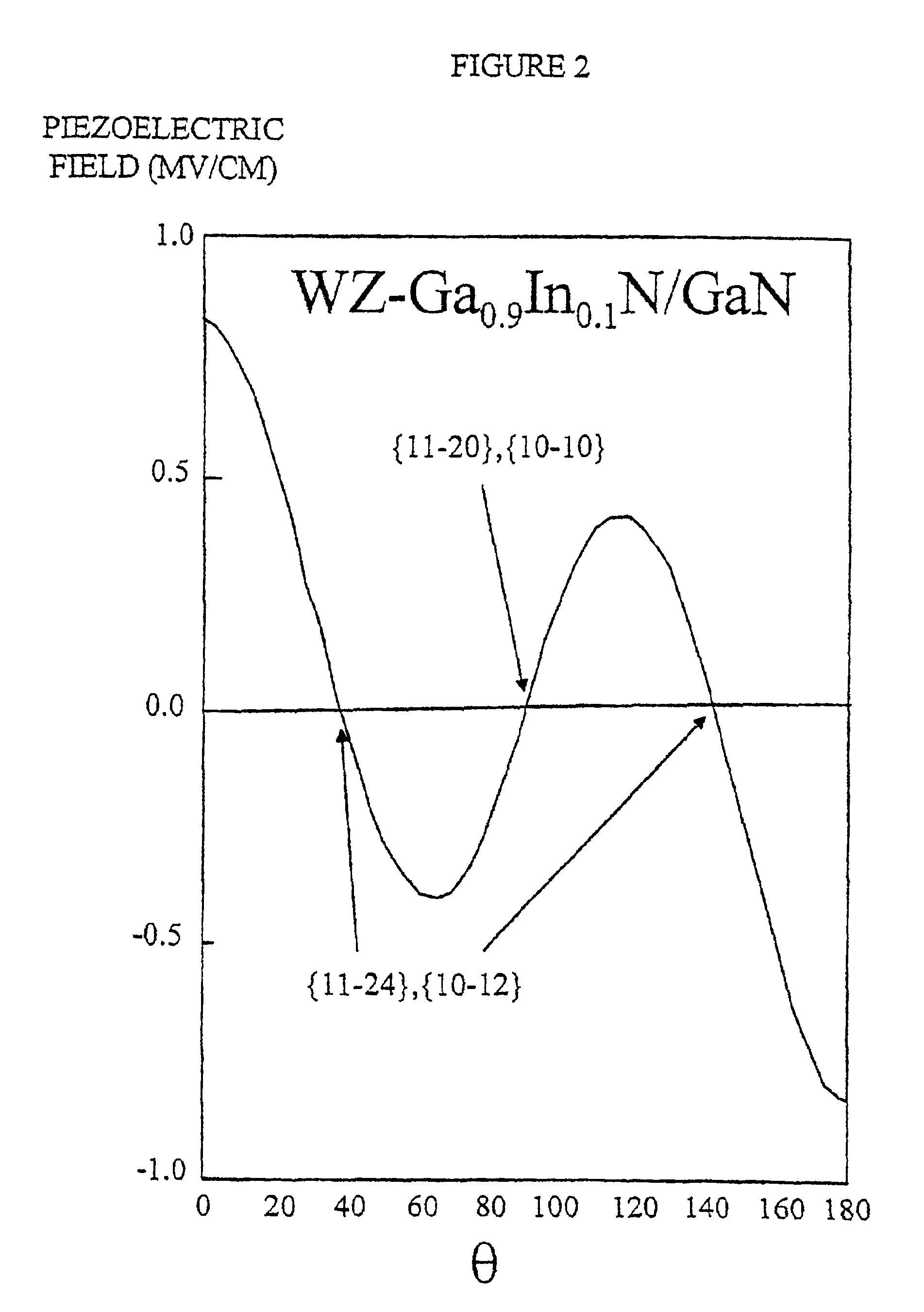
[0023]The present invention is based in part on the observation that the piezoelectric field in a strained quantum well layer depends on the orientation of the crystal structure of the quantum well layer, and hence, by controlling the facet orientation, the piezoelectric field can be minimized. The manner in which this is accomplished may be more easily understood with reference to two types of strained quantum well structures, those based on a wurtzite crystal structure and those based on a zincblende crystal structure.

[0024]Refer now to FIG. 1 which illustrates a wurtzite crystal GaN (WZ—GaN) structure 10. The piezoelectric field generated in a crystal having a facet orientation along arc 11 in FIG. 1 is shown in FIG. 2 as a function of the angle θ between the {0001} direction and the facet orientation. The data shown in FIG. 2 is for Ga0.9In0.1N strained quantu...


PUM


Abstract

A method for fabricating a light-emitting semiconductor device including a III-Nitride quantum well layer includes selecting a facet orientation of the quantum well layer to control a field strength of a piezoelectric field and/or a field strength of a spontaneous electric field in the quantum well layer, and growing the quantum well layer with the selected facet orientation. The facet orientation may be selected to reduce the magnitude of a piezoelectric field and/or the magnitude of a spontaneous electric field, for example. The facet orientation may also be selected to control or reduce the magnitude of the combined piezoelectric and spontaneous electric field strength.

Description

CROSS REFERENCE TO RELATED APPLICATIONS[0002]This is a continuation in part of U.S. patent application Ser. No. 09 / 717,647 filed on Nov. 21, 2000, now U.S. Pat. No. 6,569,704, which is a divisional of U.S. patent application Ser. No. 09 / 162,708 filed Sep. 29, 1998, now U.S. Pat. No. 6,229,151. U.S. patent application Ser. No. 09 / 717,647 and U.S. Pat. No. 6,229,151 are incorporated herein by reference in their entirety.FIELD OF THE INVENTION[0003]The present invention relates to optical semiconductor devices, and particularly, to a structure for improving the efficiency of light emitters and photodetectors fabricated from GaN-based semiconductors.BACKGROUND[0004]In the following discussion a III-N semiconductor is a semiconductor having a Group III element and nitrogen. III-N semiconductors such as GaN are useful in fabricating light emitting elements that emit in the blue and violet regions of the optical spectrum. These elements include light emitting diodes and laser diodes. Laser...

Claims


Application Information

Patent Timeline
Patent Type & Authority Patents(United States)
IPC IPC(8): H01L21/02H01L21/20H01S5/343H01L33/00H01S5/00H01S5/32H01S5/02H01L21/205H01L31/18H01L33/06H01L33/16H01L33/18H01L33/24H01L33/32
CPCB82Y20/00H01L21/02378H01L21/02389H01L21/0242H01L21/02433H01L21/02458H01L21/02502H01L21/02516H01L21/0254H01L21/02609H01L31/1844H01L31/1852H01L33/16H01L33/32H01S5/343H01S5/34333H01L21/0237Y02E10/544H01L33/0062H01L33/06H01L33/18H01L33/24H01S5/021H01S5/0213H01S5/3201H01S5/3202H01S5/32025
Inventor KRAMES, MICHAEL R.TAKEUCHI, TETSUYAYAMADA, NORIHIDEAMANO, HIROSHIAKASAKI, ISAMU
Owner LUMILEDS
Why Eureka
Try Eureka