Photomask surface defects are highly undesirable and adversely affect the resulting circuits.
Defects can result from, but not limited to, a portion of the pattern being absent from an area where it is intended to be present, a portion of the pattern being present in an area where it is not intended to be, chemical stains or residues from the
photomask manufacturing processes which cause an unintended localized modification of the
light transmission property of the
photomask, particulate contaminates such as dust,
resist flakes,
skin flakes,
erosion of the photolithographic pattern due to
electrostatic discharge, artifacts in the photomask substrate such as pits, scratches, and striations, and localized
light transmission errors in the substrate or pattern layer.
As the complexity of integrated circuits has increased, the demands on the inspection of the integrated circuits have also increased.
Both the need for resolving smaller defects and for inspecting larger areas have resulted in greater
magnification requirements and greater speed requirements.
These comparison-type inspection systems are quite expensive because they rely on pixel-by-pixel comparison of all the dies and, by necessity, rely on highly accurate methods of alignment between the two dies used at any one time for the comparison.
Apart from their high costs, this method of inspection is also unable to detect particles on opaque parts of the
reticle which have the tendency to subsequently migrate to parts that are transparent and then cause a defect on the
wafer.
Unfortunately, the edges of the pattern also cause scattering and for that reason these systems are unreliable for the detection of particles smaller than one
micrometer.
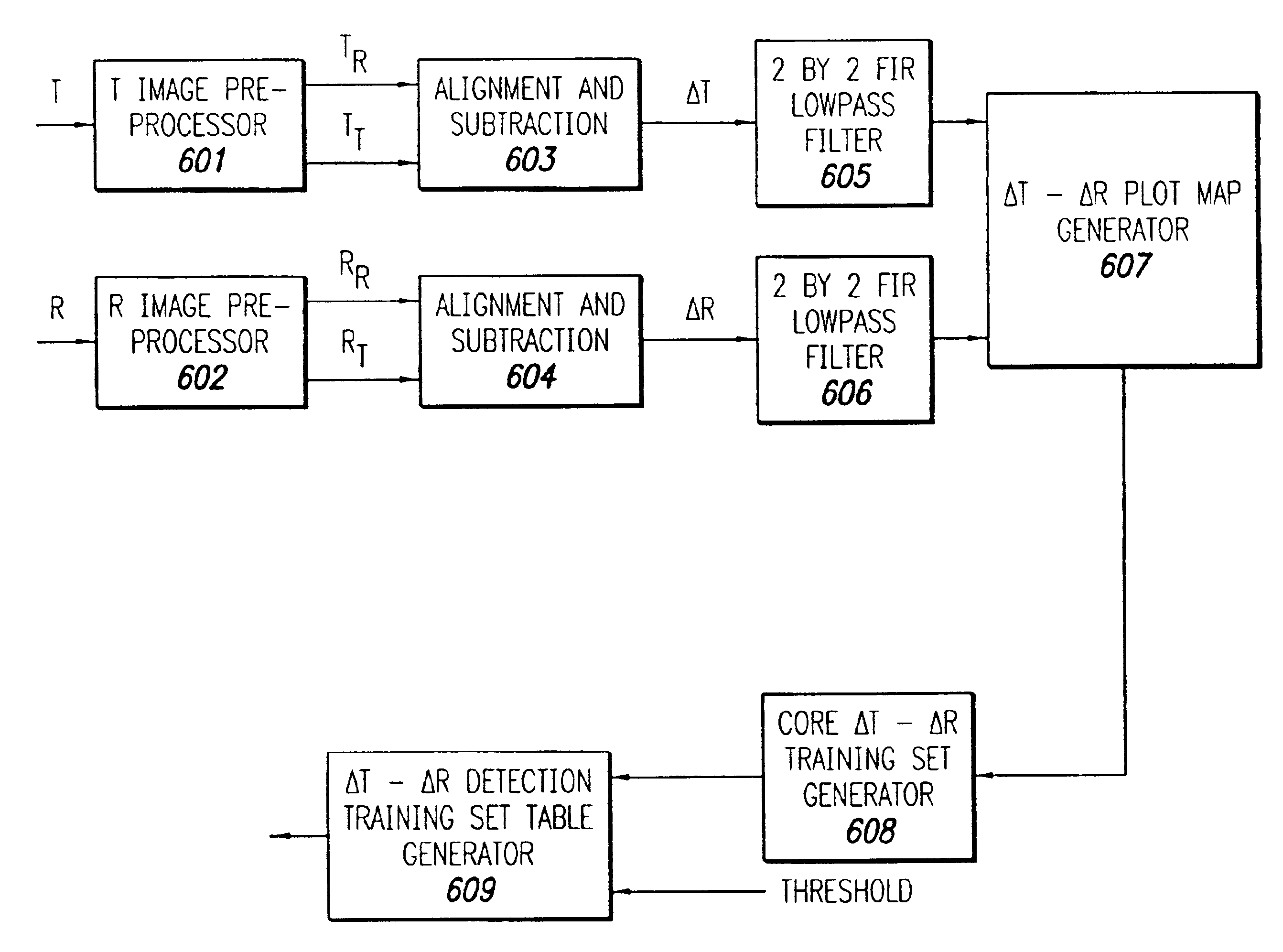
Since this system locates defects without reference or comparison to a description or image of the desired photomask pattern, it may in certain circumstances not locate defects outside of known boundaries, such as where the transmitted and reflected images differ from an expected amount by a threshold amount.
Phase defects can exist which are unwanted thickness variations created by phase etch process errors, and have similar
optical image signatures during inspection.
Hence APSM phase defects are difficult to distinguish from
design phase features using the system shown in U.S. Pat. No. 5,563,702.
Phase defects cannot be detected by this system without producing false defect readings on phase shift design features where no defects actually exist.
The difficulty with using reflected light is managing image artifacts, such as the bright chrome halos resulting from the removal of the antireflective chrome layer during
quartz etching of phase shifters.
On the other hand, use of reflected light can be problematic in the presence of image artifacts such as bright chrome halos.
During inspection, different light sources can drastically affect the quality of the information received in the presence of certain types of defects.
The phase defect
signal in brightfield
transmitted light can be substantially less than that of a similarly sized chrome defect, thereby complicating the ability to inspect the
mask.
In this method, if the difference between the pixels of the reference die and the test die exceed a predetermined value, the pixel is marked defective.
Non-defective zones used in the presence of constant thresholds have been found to be excessively large, resulting in declaring defects when no true defects exist, requiring additional post
processing.
In other words, if the non-defective zone of FIG. 3 is small, a higher probability that a defect will be located exists.
However, decreasing the non-defective zone excessively may result in too many anomalies being classified as defects.
In actuality, many errors between dies exist, including errors between test and reference dies.
If the threshold is too small, a large number of false or nuisance defects will develop, taking a great deal of time to inspect, decreasing overall
throughput.
While the system disclosed therein provides for inspection of APSMs using transmitted and reflected light, certain defects may exist that may not be picked up by the Emery design.
Further, the Emery design may require inspection of areas that are flagged as defective or potentially defective, potentially decreasing overall speed and
throughput.

