
Substrate processing apparatus and substrate processing method

a substrate processing and processing apparatus technology, applied in the direction of instruments, photosensitive materials, furnaces, etc., can solve problems such as poor processing efficiency, and achieve the effect of improving processing efficiency

Inactive Publication Date: 2005-02-08
TOKYO ELECTRON LTD
View PDF4 Cites 47 Cited by
  • Summary
  • Abstract
  • Description
  • Claims
  • Application Information

AI Technical Summary

Benefits of technology

An object of the present invention is to provide a substrate processing apparatus and a substrate processing method in which the throughput is improved.
According to the aforementioned structure of the present invention, the substrate, which is subjected to the next light-exposure process, is positioned before the light-exposure process unit at the time of ending the light-exposure process of the substrate in the light-exposure process unit. This makes it possible to shorten the time required for loading the substrate, which is subjected to the next light-exposure process after the end of the light-exposure process, into the light-exposure process unit. This also makes it possible to shorten the entire process time and to improve the throughput.

Problems solved by technology

This causes a problem in which the throughput becomes worse.

Method used


Image

  • Substrate processing apparatus and substrate processing method
  • Substrate processing apparatus and substrate processing method
  • Substrate processing apparatus and substrate processing method

Examples


Embodiment Construction

Hereinbelow, a preferred embodiment of the present invention will be described with reference to the drawings.

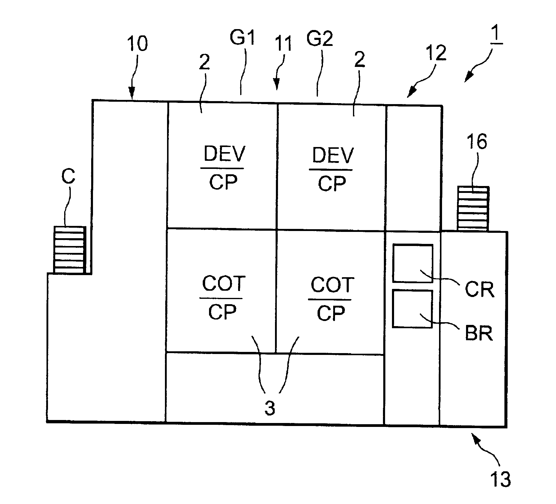
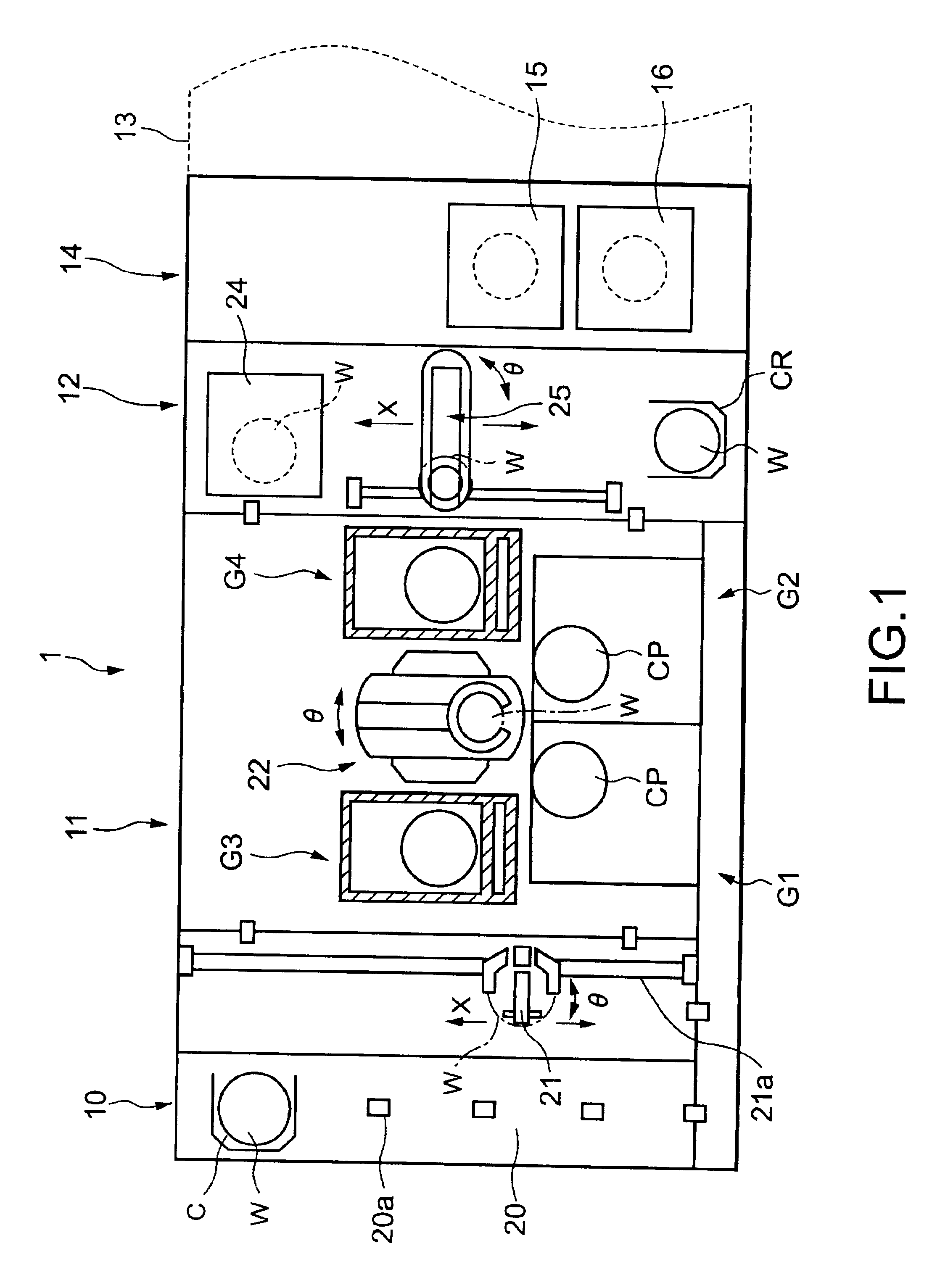
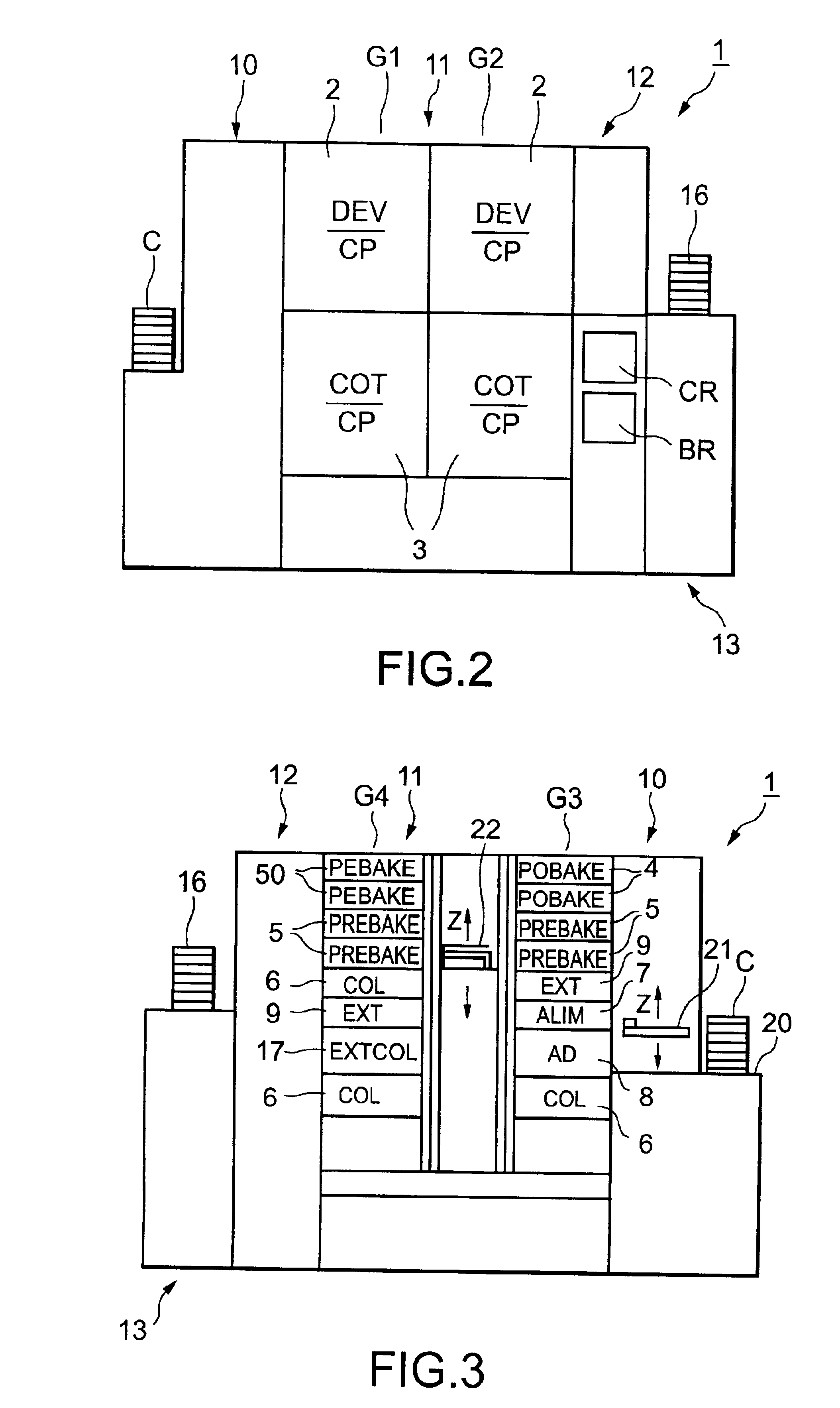
FIG. 1 is a plane view showing a coating and developing process system according to one embodiment of the present invention; FIG. 2 is a front view showing the coating and developing process system shown in FIG. 1; and FIG. 3 is a rear view showing the coating and developing process system shown in FIG. 1.

As shown in FIGS. 1 through 3, a coating and developing process system 1 is constituted by integrally connecting a cassette station 10, a process station 11, an interface section 12, and a wafer delivering section 14. The cassette station 10 externally loads wafers W into the system 1 in units of a plurality of, e.g., 25 wafers for a wafer cassette C, and unloads them from the system externally. Also, the wafers W are loaded and unloaded in / from the wafer cassette. In the process station 11, various single-process units, which provide predetermined processes to wafers one b...


PUM


Abstract

Transferring apparatus control means movement of a transferring apparatus for transferring a wafer to a resist liquid coating unit from a cooling process unit. A storage section of the transferring apparatus controller stores a coating time required for a resist film coating and a moving time required for the transfer of the wafer. When a coating start time of a resist film is inputted, the control section calculates a coating end time from the stored coating time. Further, the control section calculates time of taking out a wafer W, which is next subjected to a coating process from the cooling process unit, from the coating end time and the stored moving time. Based on the calculated time, the transferring apparatus controller instructs the transferring apparatus about timing to take out the wafer. This makes it possible to improve the throughput.

Description

BACKGROUND OF THE INVENTION1. Field of the InventionThe present invention relates to a substrate processing apparatus and a substrate processing method wherein a to-be-processed object such as a semiconductor wafer and the like is cooled by a cooling process unit in a resist film coating process and the cooled object is transferred to a resist liquid coating unit from the cooling process unit.2. Description of the Related ArtIn a semiconductor device manufacturing process, the photolithography technique is used. In this photolithography technique, a resist coating is applied on the surface of a semiconductor wafer (hereinafter simply referred to “wafer”), and the coated surface is exposed to light and developed to have a predetermined pattern. Since these processes of resist coating, light-exposure, and developing are carried out at about room temperature, a cooling process is carried out such that the temperature of the wafer is set to be substantially room temperature before these...

Claims


Application Information

Patent Timeline
IPC IPC(8): B65G49/07G03D5/00H01L21/00H01L21/027
CPCH01L21/67276Y10S414/135H01L21/027
Inventor OKUBO, KENICHIKANBAYASHI, AKIRA
Owner TOKYO ELECTRON LTD
Features
  • Generate Ideas
  • Intellectual Property
  • Life Sciences
  • Materials
  • Tech Scout
  • Unparalleled Data Quality
  • Higher Quality Content
  • 60% Fewer Hallucinations
Learn More