Light-emitting semiconductor device using gallium nitride compound semiconductor

a technology of compound semiconductors and light-emitting devices, which is applied in the direction of semiconductor devices, electrical devices, nanotechnology, etc., can solve the problems of insufficient optimization of the conditions for emitted light, insufficient luminous efficiency, and persisting problems, so as to improve the luminous efficiency of the light-emitting device

Inactive Publication Date: 2005-02-08
TOYODA GOSEI CO LTD
View PDF35 Cites 16 Cited by
  • Summary
  • Abstract
  • Description
  • Claims
  • Application Information

AI Technical Summary

Benefits of technology

[0011]An object of the present invention is to improve luminous efficiency of a light-emitting device using gallium nitride compound semiconductor.

Problems solved by technology

However, a problem persists in luminous efficiency.
In the conventional light-emitting devices using gallium nitride compound semiconductor, conditions for emitting light are not always optimized.

Method used


Image

  • Light-emitting semiconductor device using gallium nitride compound semiconductor
  • Light-emitting semiconductor device using gallium nitride compound semiconductor
  • Light-emitting semiconductor device using gallium nitride compound semiconductor

Examples


first embodiment

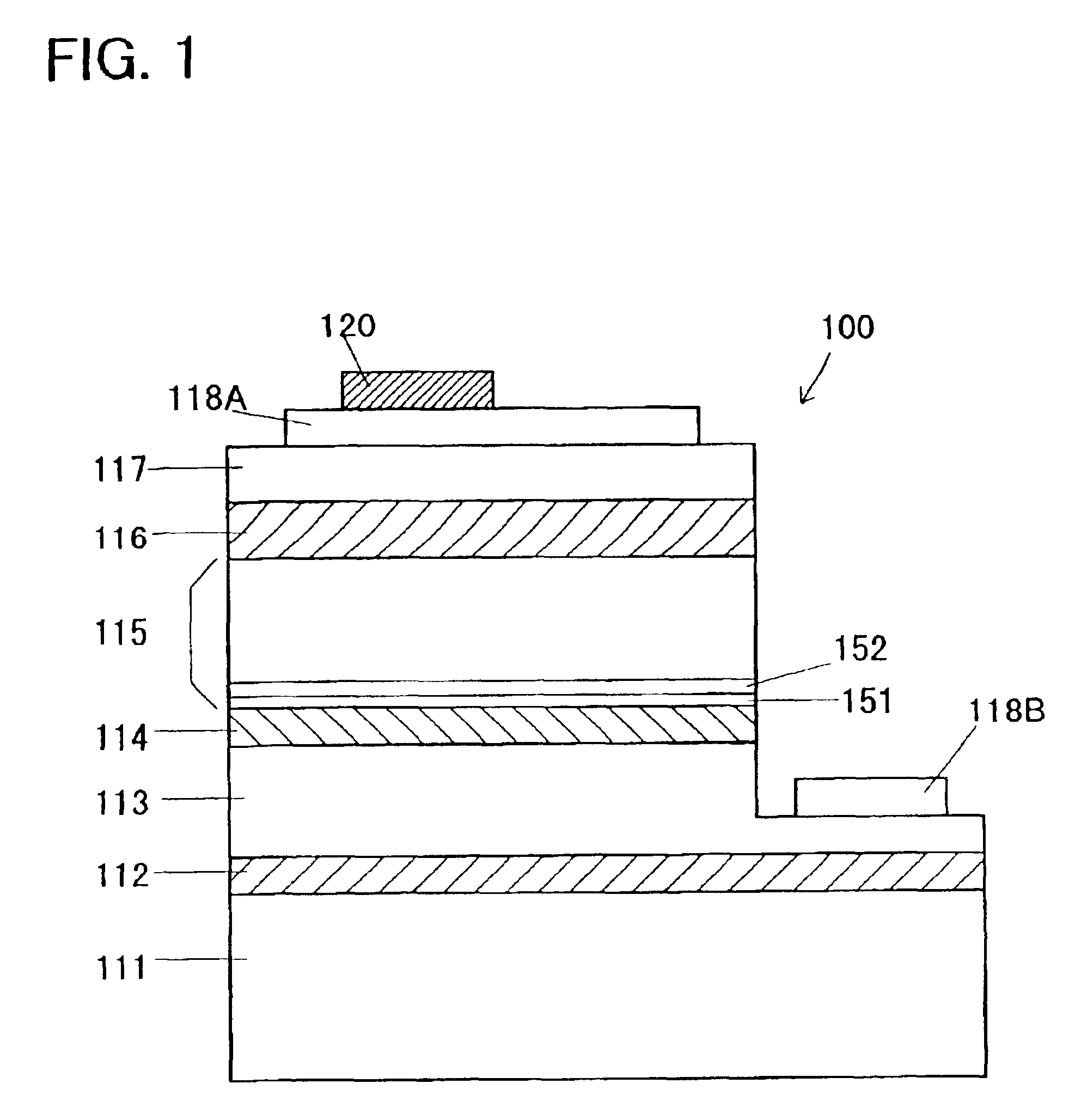
[0047](First Embodiment)

[0048]FIG. 1 illustrates a sectional view of a light-emitting device 100 using gallium nitride (GaN) compound semiconductor formed on a sapphire substrate 111. The light-emitting device 100 has a sapphire substrate 111 which has a buffer layer 112 made of nitride aluminum (AlN) having a thickness of 25 nm and an n-cladding or an n-contact layer (n+-layer) 113 made of silicon (Si) doped GaN and having a thickness of 3000 nm successively thereon.

[0049]And a strain relaxation layer 114 made of a non-doped In0.03Ga0.97N having a thickness of about 180 nm is formed on the n-cladding layer or the n-contact layer (n+-layer) 113. The strain relaxation layer 114 functions to relax a stress to an emission layer 115, generated by the difference between thermal expansion coefficients of the sapphire substrate 111 and the emission layer 115.

[0050]An emission layer 115 is constructed with a multi quantum-well (MQW) structure, which is made of six barrier layers 151 made of...

second embodiment

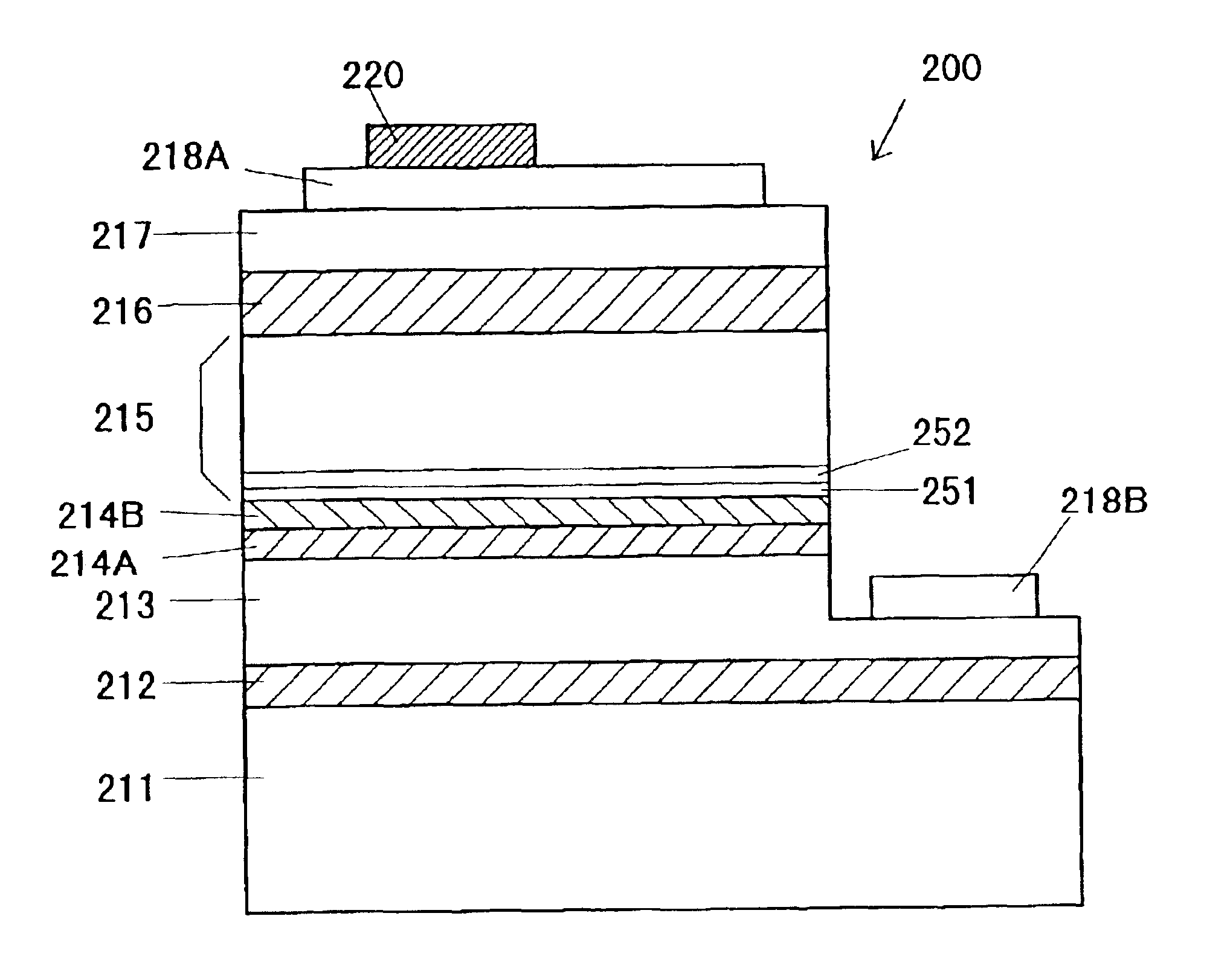
[0077](Second Embodiment)

[0078]FIG. 4 illustrates a sectional view of a light-emitting device 200 using gallium nitride (GaN) compound semiconductor formed on a sapphire substrate 211. The light-emitting device 200 has a sapphire substrate 211 which has a buffer layer 212 made of nitride aluminum (AlN) having a thickness of 25 nm and an n-contact layer 213 made of silicon (Si) doped GaN and having a thickness of 3 μm successively thereon.

[0079]And a strain relaxation layer 214A made of a non-doped In0.03Ga0.97N having a thickness of about 180 nm is formed on the n-contact layer 213. The strain relaxation layer 214A functions to relax a stress to an emission layer 215, generated by the difference between thermal expansion coefficients of the sapphire substrate 211 and the emission layer 215. And an n-cladding layer 214B made of a silicon (Si) doped Al0.05Ga0.95N having a thickness of about 200 nm is formed on the strain relaxation layer 214A.

[0080]An emission layer 215 is constructed...

third embodiment

[0108](Third Embodiment)

[0109]FIG. 7 illustrates a sectional view of a light-emitting device 300 using gallium nitride (GaN) compound semiconductor formed on a sapphire substrate 311. The light-emitting device 300 has a sapphire substrate 311 which has a buffer layer 312 made of nitride aluminum (AlN) having a thickness of 25 nm and an n-contact layer 313 made of silicon (Si) doped GaN and having a thickness of 3 μm successively thereon.

[0110]And a strain relaxation layer 314A made of a non-doped In0.03Ga0.97N having a thickness of about 180 nm is formed on the n-contact layer 313. The strain relaxation layer 314A functions to relax a stress to an emission layer 315, generated by the difference between thermal expansion coefficients of the sapphire substrate 311 and the emission layer 315. And an n-cladding layer 314B made of a silicon (Si) doped Al0.05Ga0.95N having a thickness of about 200 nm is formed on the strain relaxation layer 314A.

[0111]An emission layer 315 is constructed ...


PUM

PropertyMeasurementUnit
thicknessaaaaaaaaaa
thicknessaaaaaaaaaa
wavelengthaaaaaaaaaa

Abstract

A barrier layer made of AlxGa1-xN (0<x≦0.18) is formed in a light-emitting semiconductor device using gallium nitride compound having a multi quantum-well (MQW) structure. By controlling a composition ratio x of aluminum (Al) or thickness of the barrier layer, luminous intensity of the device is improved.
An n-cladding layer made of AlxGa1-xN (0<x≦0.06) is formed in a light-emitting semiconductor device using gallium nitride compound. By controlling a composition ratio x of aluminum or thickness of the n-cladding layer, luminous intensity of the device is improved.
A p-type layer and an n-type layer are formed in a light-emitting semiconductor device using gallium nitride compound having a double-hetero junction structure. By controlling a ratio of a hole concentration of the p-type layer and an electron concentration of the n-type layer approximates to 1, luminous intensity of the device is improved.

Description

[0004]This is a Divisional application of U.S. application Ser. No. 09 / 394,527, which was filed on Sep. 10, 1999, now U.S. Pat. No. 6,423,984 and whose contents are incorporated in their entirety by reference.BACKGROUND OF THE INVENTION[0005]1. Field of the Invention[0006]The present invention relates to a light-emitting device using gallium nitride compound semiconductor whose luminous efficiency is improved. Especially, the present invention relates to the device which emits the ultraviolet ray.[0007]2. Description of the Related Art[0008]A conventional light-emitting device, which have layers made of gallium nitride compound semiconductor laminated on a substrate, is known to have the following structure. The device has a sapphire substrate, and on the sapphire substrate the following layers are formed sequentially: a buffer layer made of aluminum nitride (AlN); an n-cladding and / or an n-contact layer of high carrier concentration, which is made of a silicon (Si) doped GaN of n-t...

Claims


Application Information

Patent Timeline
Patent Type & Authority Patents(United States)
IPC IPC(8): H01L33/00H01L33/06H01L33/32
CPCB82Y20/00H01L33/06H01L33/32
Inventor KATO, HISAKIWATANABE, HIROSHIKOIDE, NORIKATSUASAMI, SHINYA
Owner TOYODA GOSEI CO LTD
Why Eureka
Try Eureka