Variable angle illumination wafer inspection system

a wafer inspection and variable angle technology, applied in the field of wafer inspection systems, can solve the problems of inability to penetrate the light between dense lines, roughness and graininess of other materials, and less useful than normal illumination for some layers, etc., and achieve the effect of optimizing the inspection characteristics of a scanned layer

Inactive Publication Date: 2005-02-08
APPLIED MATERIALS INC
View PDF23 Cites 49 Cited by
  • Summary
  • Abstract
  • Description
  • Claims
  • Application Information

AI Technical Summary

Benefits of technology

An advantage of the present invention is a wafer inspection system selectively and advantageously permitting use of normal scanning illumination or oblique scanning illumination to optimize the inspection characteristics of a scanned layer.
According to the present invention, the foregoing and other advantages are achieved in part by a variable illumination angle substrate inspection system. The variable illumination angle substrate inspection system comprises: a light source providing a light beam; a scanner imparting scanning deflection to the light beam to provide scanning beam approaching the substrate at a first angle; and a deflection element selectively insertable into optical path of the scanning beam and deflecting the scanning beam so as to approach the substrate at a second angle.
Another aspect of the present invention is a variable illumination angle inspection system for inspecting a substrate including a light source providing a light beam and a scanning element adapted to output the light beam along a first optical path to the substrate, the first optical path including a portion incident t...

Problems solved by technology

All of these conventional approaches have advantages and disadvantages, some of which relate to the particular application or situation in which the system is used.
Some layers (such as bare silicon) are very smooth whereas some others (such as deposited aluminum) can be very rough and grainy.
Oblique illumination angles have, however, some limitations which make them less useful than normal illumination for some layers.
One deficiency of oblique illumination angles is the inability of...

Method used


Image

  • Variable angle illumination wafer inspection system
  • Variable angle illumination wafer inspection system
  • Variable angle illumination wafer inspection system

Examples


Embodiment Construction

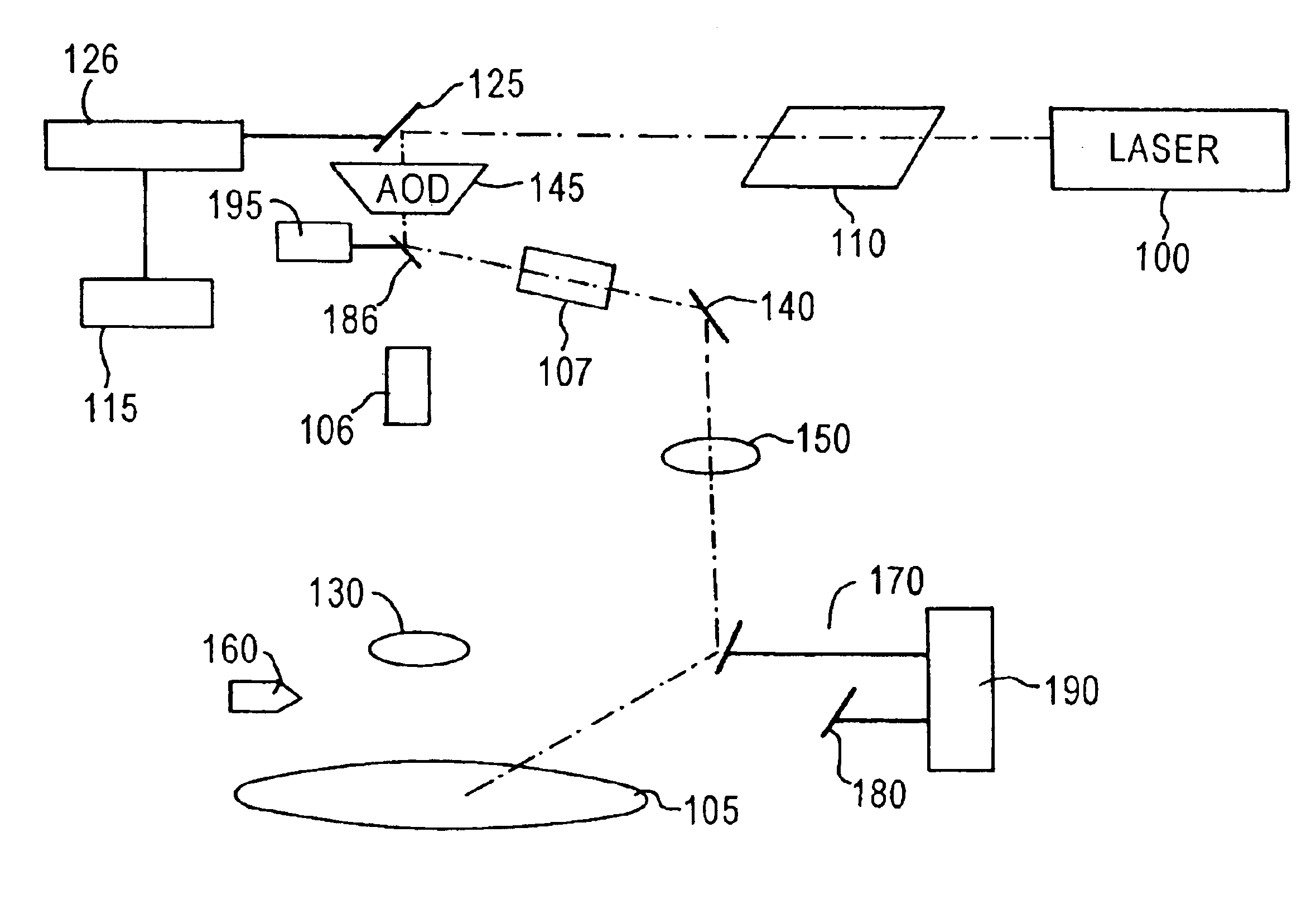
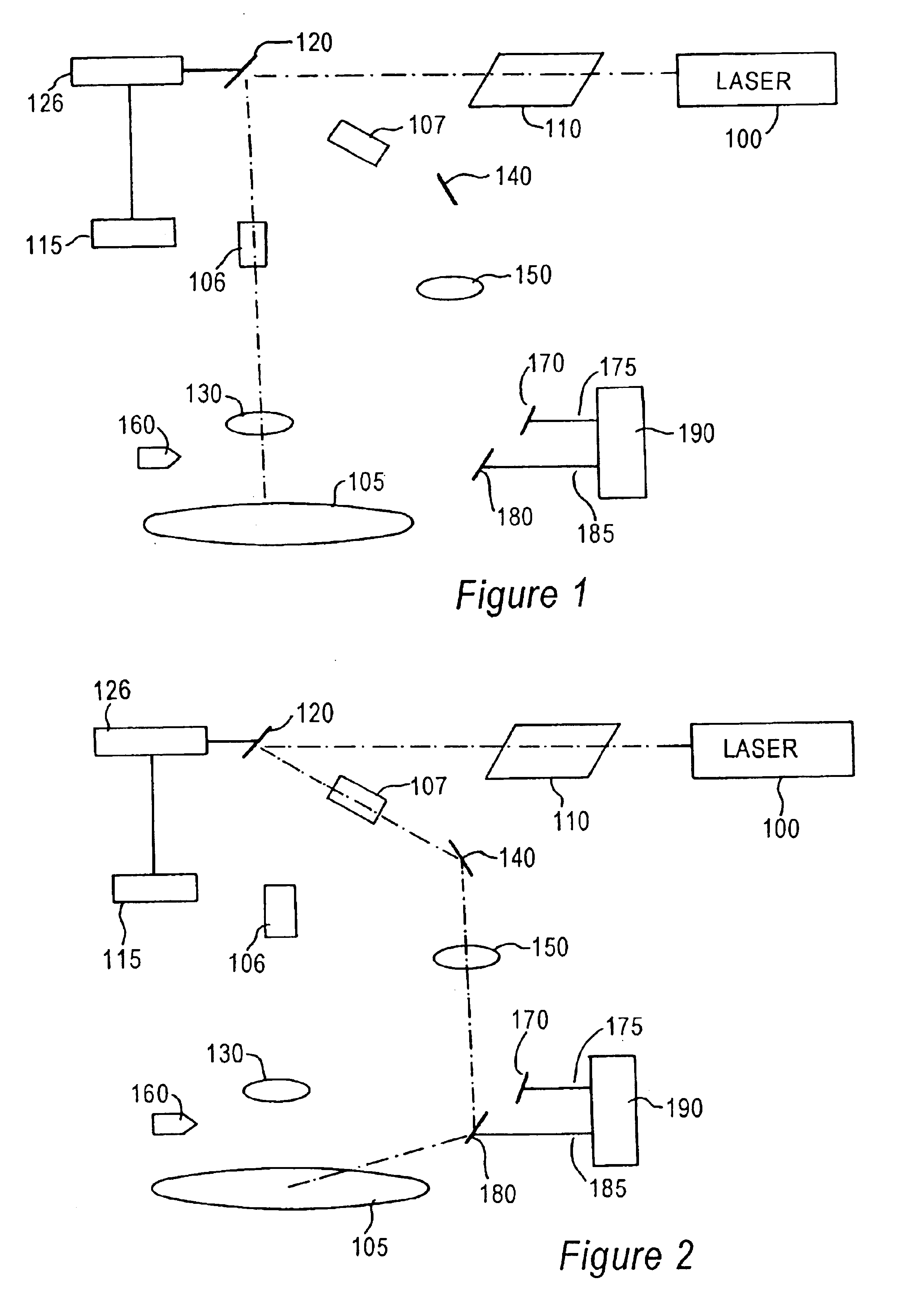
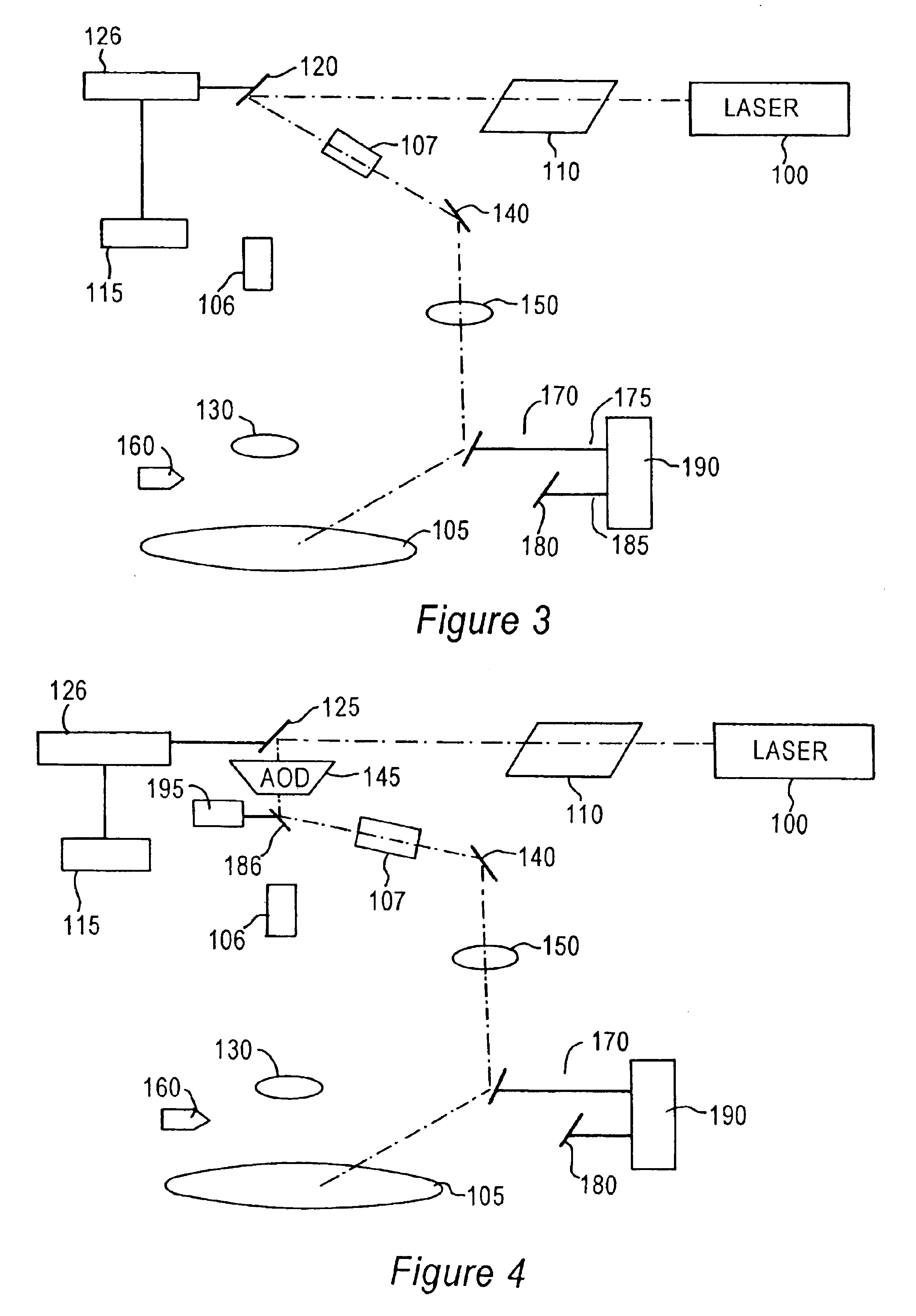
FIG. 1 illustrates a first embodiment of the invention. Laser 100, such as an argon laser or other suitable high intensity laser beam source, provides a light beam which is used to scan the surface of a semiconductor wafer or substrate 105 held by a vacuum chuck. Conventional optics 110 are used to shape the light beam and may include, for example, a beam expander and cylindrical lenses (not shown). The foregoing components and their principles of operation are well-known and are therefore not described herein in detail.

A mechanism for scanning the laser beam is provided. This mechanism for scanning the laser beam may include, as well known in the art, a galvanometric scanning planar mirror, a rotating polygon mirror, an acousto-optic deflector (AOD), or any other mechanism for imparting the requisite laser scan motion to the laser beam, wherein this mechanism is represented in FIG. 1 by reference numeral 120 and is hereinafter referred to equally as scanning element 120. Additional...


PUM


Abstract

A variable illumination angle inspection system is provided, including a light source providing a light beam and a scanner imparting scanning deflection to the light beam to provide a scanning beam approaching a substrate at a first angle. A deflection element is selectively insertable into an optical path of the scanning beam to deflect the scanning beam so as to cause the scanning beam to approach the substrate at a second angle.

Description

BACKGROUND OF THE INVENTIONWafer inspection systems are well known in the art. One conventional system, embodied in U.S. Pat. No. 5,699,447 uses normal illumination and bright-field detection (i.e., the illumination approaches the wafer at ninety degrees thereto). Another type of conventional system, as embodied in U.S. Pat. No. 5,825,482 uses oblique illumination and dark-field detection (i.e., the illumination approaches the wafer obliquely). A third type of system, as embodied in U.S. Pat. No. 5,982,921, uses normal illumination and dark field detection. All of these conventional approaches have advantages and disadvantages, some of which relate to the particular application or situation in which the system is used.Under normal illumination, the surface of the object viewed is normal to the optic axis of the objective lens and light is used to illuminate the object. In a bright field system, light reflected back to the objective lens in a direction substantially parallel to the i...

Claims


Application Information

Patent Timeline
IPC IPC(8): G01N21/21G02B26/10G01N21/88G01N21/95G02B21/08G02B21/06
CPCG01N21/21G02B26/10G02B21/082G01N21/9501
Inventor ALMOGY, GILADMAZAKI, HADARPHILLIP, ZVI HOWARDREINHORN, SILVIUGOLDBERG, BORISSOME, DANIEL I.
Owner APPLIED MATERIALS INC
Why Eureka
Try Eureka