Chemical monolayer memory device

a memory device and monolayer technology, applied in the manufacture of electrode systems, record information storage, optical radiation measurement, etc., to achieve the effect of enhancing the efficiency of electron emission

Inactive Publication Date: 2005-02-15
THE OHIO STATE UNIV RES FOUND
View PDF6 Cites 28 Cited by
  • Summary
  • Abstract
  • Description
  • Claims
  • Application Information

AI Technical Summary

Benefits of technology

The present invention also includes field emitter devices, analogous to those that are the basis of flat panel displays. In these devices, the chemical monolayers of the present invention serve to enhance the efficiency of electron emission in response to applied potential. Electrons emitting from the monolayer may be allowed to strike a light emitter such as a fluorophore-containing surface. These devices may be used to create flat panel displays and screens.
The present invention may also include any combination of molecular circuit components and devices described above by selecting molecular unit types and constructing arrangements or arrays to take advantage of the respective functional character of each type or array of types of monolayers. For instance, depending upon the desired application, one may provide, for instance:1. Separate regions of differing and discreet molecular unit type construction in accordance with any of the functions described herein (e.g. one region to bind iron ions and another to bind copper ions; or one region sensitive to one EM frequency and another sensitive to another EM fr

Problems solved by technology

Naturally, depending on the degree of conductivity of the monolayer and its constituent molecular units, the monolayer junctions and devices may tolerate greater or l

Method used


Image

  • Chemical monolayer memory device
  • Chemical monolayer memory device
  • Chemical monolayer memory device

Examples


Embodiment Construction

)

In accordance with the foregoing summary, the following presents a detailed description of the preferred embodiment of the invention that is currently considered to be the best mode.

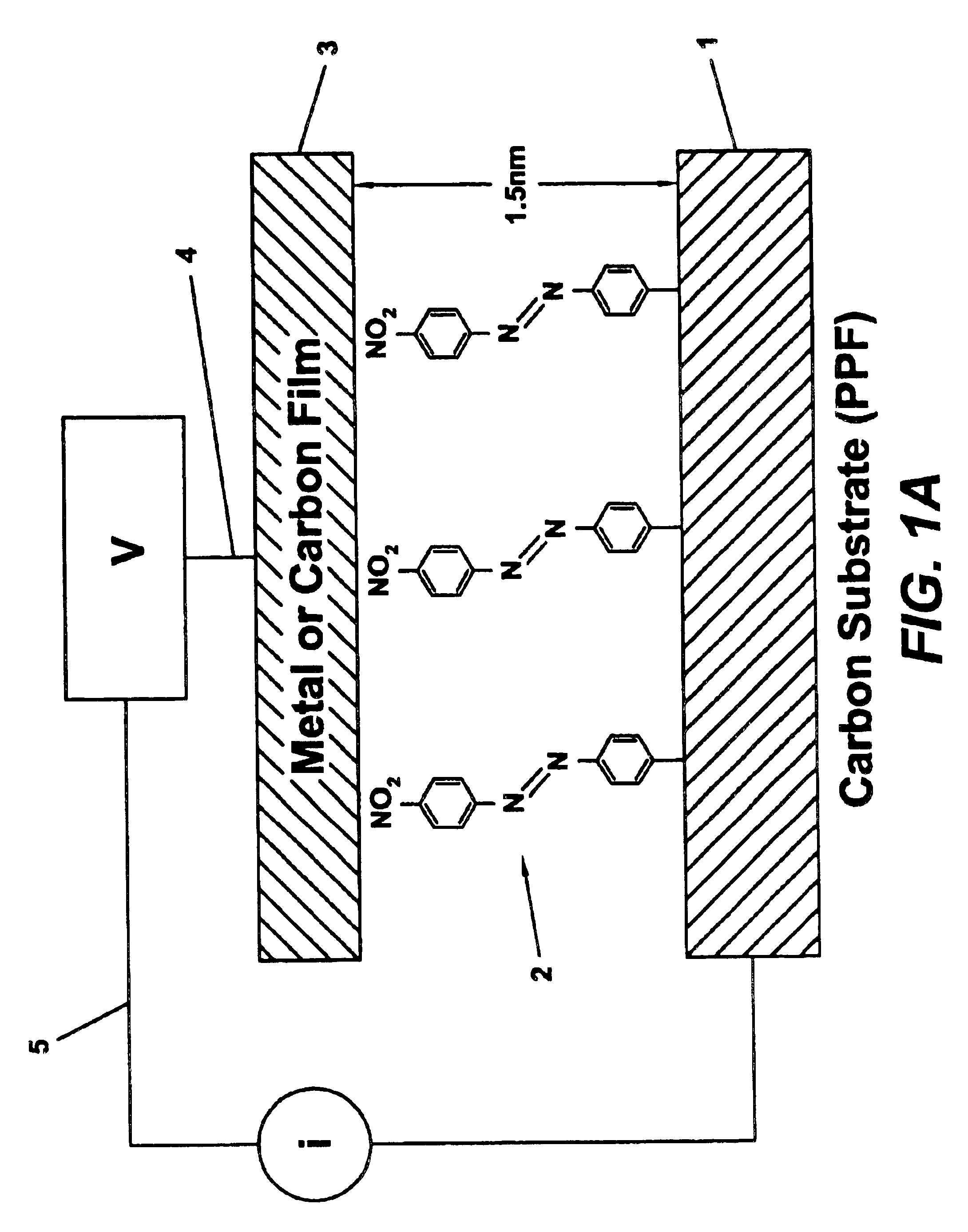
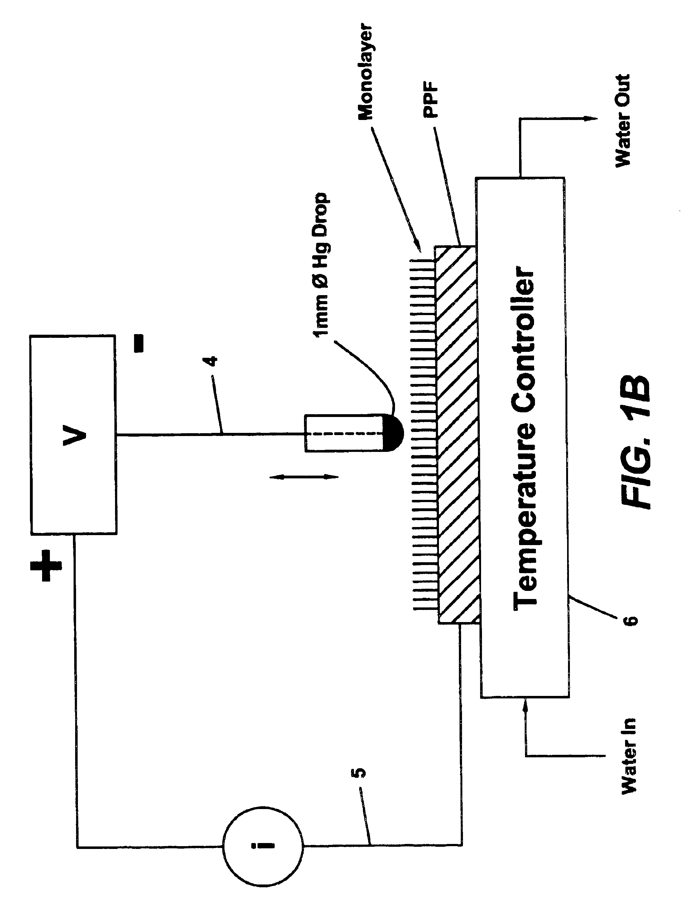
FIG. 1 shows a schematic of a microelectronic junction in accordance with one embodiment of the present invention. FIG. 1 shows a first conductive member 1 or substrate such as a carbon pyrolyzed photoresist film (“PPF”). To this first conductive member 1 is attached a single layer of a plurality of nitroazobenzene molecules (the “chemical monolayer”), covalently bonded to the carbon PPF. The chemical monolayer 2 is disposed between the first conductive member 1 and the second conductive member 3 (i.e. a liquid such as a mercury drop in a device shown in FIG. 1A), with a layer thickness as small as about 1.5 nm. Covalent bonding between the PPF film and the carbon leads to strong, electronic coupling between the molecular monolayer and the carbon PPF. In a finished device, the second conductive member 3...


PUM


Abstract

The present invention includes a chemical monolayer construction that comprises: (a) a substrate having a contact surface; and (b) a plurality of substantially parallel molecular units, wherein said molecular units are attached to said substrate so as to be strongly coupled electronically to said substrate, such as through a conjugated bond. The present invention also includes electronic circuit components and devices including a chemical monolayer construction of the present invention.

Description

TECHNICAL FIELD OF THE INVENTIONThe present invention is in the field of chemical monolayers and microelectronic junctions, and includes chemical sensors, photosensors and other devices containing them.BACKGROUND OF THE INVENTIONThe term “molecular electronics” has been used to describe phenomena or devices that include a molecule as a circuit element (1,2). The motivation for the field is the prospect of making extremely small (potentially one molecule) electronic components with a much wider range of functions than conventional semiconductor electronic devices. If molecular devices become practical, a wide variety of applications in microelectronics, computing, imaging and display technology and chemical sensing can be envisioned. The large majority of proposed molecular electronic devices are based on the Gold-thiol system (Au / thiol), in which organic mercaptans “self assemble” on a flat gold surface to form an ordered monomolecular layer (3-6). In many cases, scanning tunneling ...

Claims


Application Information

Patent Timeline
IPC IPC(8): G11B9/00G01N27/12B82B1/00C30B29/00G01J1/02G11B5/127G11B5/33H01J9/02H01J29/04H01J31/12H01L29/06H01L29/12H01L29/66H01L51/05H01L51/42
CPCB82Y10/00G11B9/14G11B9/1472G11C11/14H01L51/0595G11B9/149B05D1/185Y10T428/268Y10T428/261Y10T428/31536Y10T428/31504G11B9/04H10K10/701
Inventor MCCREERY, RICHARD L.
Owner THE OHIO STATE UNIV RES FOUND
Why Eureka
Try Eureka