Objective lens for an electron microscopy system and electron microscopy system

a technology of electron microscopy and objective lens, which is applied in the field of electron microscopy system, can solve the problems of putting specific demands on the electron microscopy system, increasing the number of complex and powerful devices, and increasing the number of optical instruments, so as to reduce overlap, reduce the effect of distance and larger working distan

Inactive Publication Date: 2005-02-15
CARL ZEISS NTS GMBH
View PDF15 Cites 126 Cited by
  • Summary
  • Abstract
  • Description
  • Claims
  • Application Information

AI Technical Summary

Benefits of technology

[0029]Basically, the geometry and arrangement of the components of the conventional objective lens were changed in order to be able to, according to a first aspect, reduce the angle between the conical outer pole shoe and the z-axis and thus to reduce the space required for the objective lens and thus the space required for the electron-microscopic system. As a result, a substantially two-dimensionally extended object can be tilted to a greater extent relative to the optical axis of the electron microscopy system.
[0067]The electron microscopy system and the ion beam processing system are positioned relative to each other such that their optical axes substantially intersect in a plane defined by a surface of the object to be examined. The object is held by an object support which enables a defined orientation of the object in front of the electron microscopy system and the ion beam processing system. As a result, the angle at which the focused ion beam and the focused electron beam impinge on the object surface can be adjusted in a defined angle range. As a result, it is, for example, possible to generate holes and trenches with side walls of different steepness. In particular, the ion beam can be positioned vertically in respect of the object and thus allows the production of trenches with vertical side walls which are of great importance for certain applications.

Problems solved by technology

In particular, in semiconductor technology there is a demand for ever smaller, more complex and powerful devices.
With increasing wafer size, this puts specific demands on the electron microscopy system.
Accordingly, in a system comprising such a conventional objective lens it is not possible to cut trenches with vertical walls into an object by means of the FIB and at the same time to carry out imaging through the electron microscope.
When the electron microscopy system and the focused ion beam are simultaneously operated, a magnetic field generally needs to be minimized in the region of the object manipulated by the ion beam, because the ions are deflected by the magnetic field which results in an impairment of the processing accuracy of the focused ion beam.
Moreover, in such a magnetic field the ion beam may be split into isotopes which might even fully exclude its usability.

Method used


Image

  • Objective lens for an electron microscopy system and electron microscopy system
  • Objective lens for an electron microscopy system and electron microscopy system
  • Objective lens for an electron microscopy system and electron microscopy system

Examples


Embodiment Construction

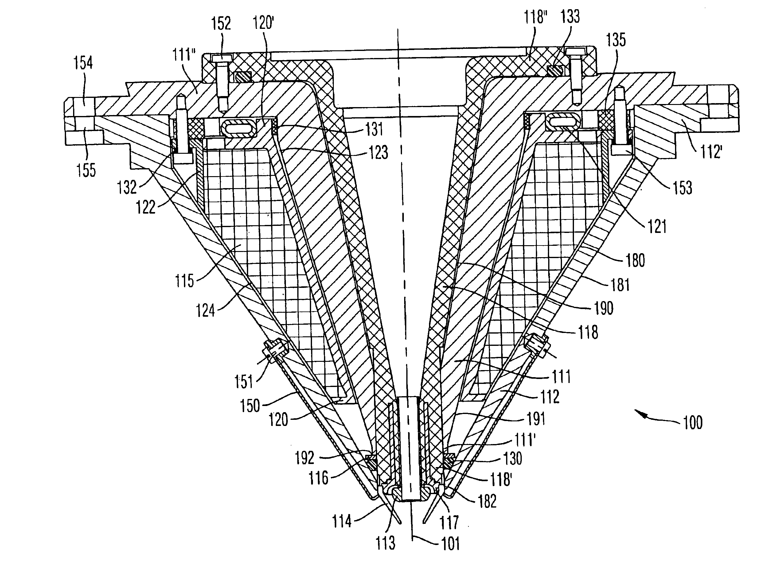
[0077]An objective lens 100 shown in FIGS. 3, 4 and 5 serves to focus an electron beam in an electron microscopy system. The objective lens 100 comprises a magnetic lens as well as an electrostatic lens. Accordingly, the focusing is effected both electrostatically and magnetically. The electrostatic lens also serves to decelerate the electrons of the primary electron beam. The magnetic lens comprises a pole shoe arrangement with an inner pole shoe 111 and an outer pole shoe 112. Both pole shoes 111, 112 are formed to rotationally symmetrically surround a central optical axis 101, i.e., the beam path of a primary electron beam.

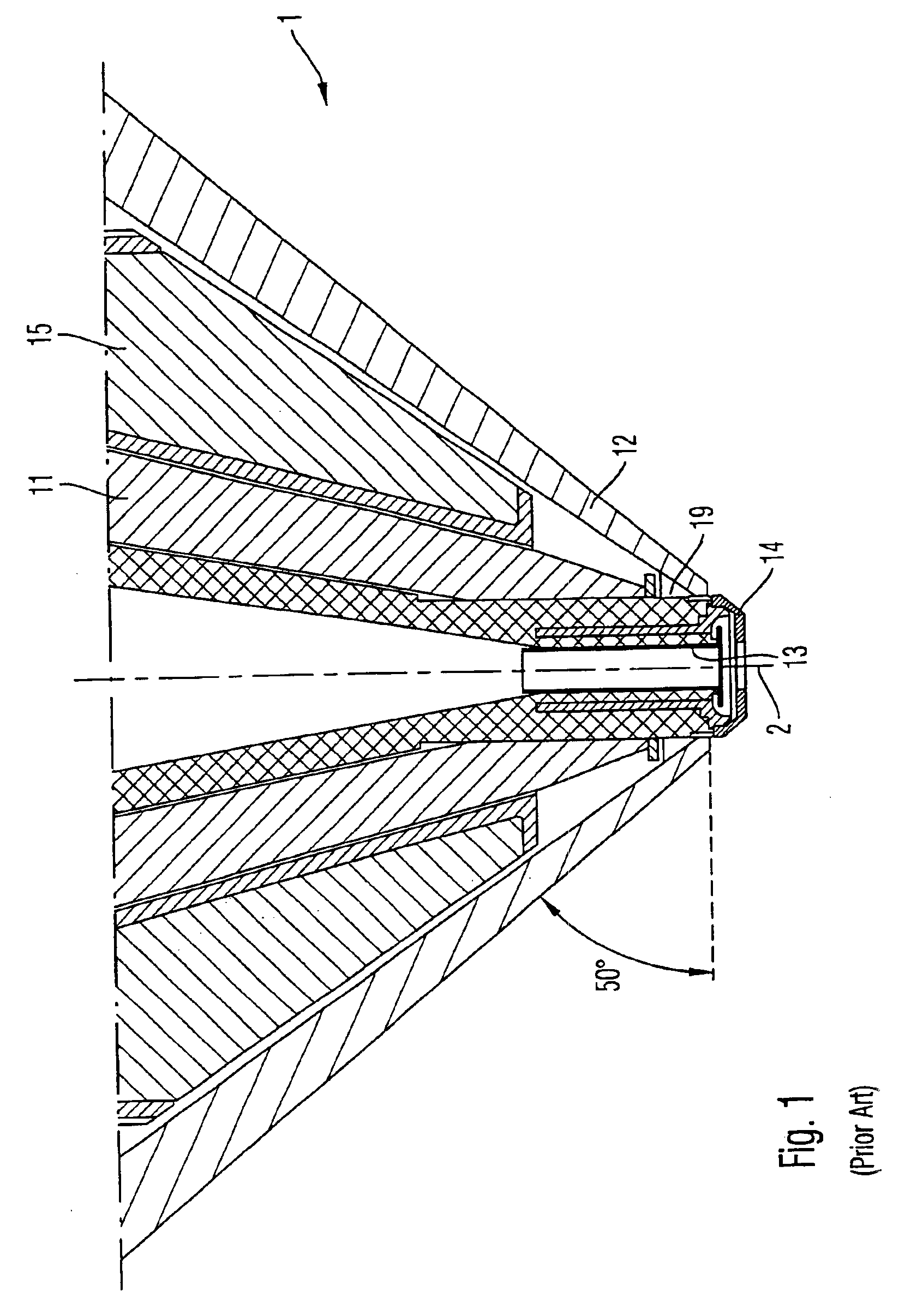
[0078]The inner pole shoe 111 is, in z-direction, of substantially conical shape and tapers in this cone-shaped region continuously towards the object plane. In a lowermost region in z-direction of the inner pole shoe 111, the latter comprises a hollow-cylindrical region 111′ which extends over about 2.2 mm in z-direction. The inner side 190 of the inner pole s...


PUM


Abstract

An objective lens with magnetic and electrostatic focusing for an electron microscopy system is provided whose at least partially conical outer shape allows orienting an object to be imaged at a large angle range in respect of an electron beam, said objective lens exhibiting, at the same time, good optical parameters. This is enabled by a specific geometry of the lens elements. Furthermore, an examination for the simultaneous imaging and processing of an object is proposed which comprises, besides an electron microscopy system with the above-mentioned objective lens, also an ion beam processing system and an object support.

Description

BACKGROUND OF THE INVENTION[0002]1) Field of the Invention[0003]The invention relates to an electron microscopy system with magnetic and electrostatic focusing and, in particular, to an objective lens for such a system. Furthermore, the invention relates to an examination system for imaging and manipulating an object, said examination system comprising such an electron microscopy system.[0004]2) Brief Description of Related Art[0005]In many technical fields and applications there is an increasing trend towards miniaturization. In particular, in semiconductor technology there is a demand for ever smaller, more complex and powerful devices. There is thus a demand, for example, in quality assurance and process analysis, to enable an optical inspection of the wafer as well as of devices being produced thereon and of the finished devices, respectively. Since the size of the individual structures of the devices is in the micrometer range and below, usually electron microscopes are used to...

Claims


Application Information

Patent Timeline
Patent Type & Authority Patents(United States)
IPC IPC(8): H01J37/10H01J37/145H01J37/141H01J37/28H01J37/317
CPCH01J37/145H01J2237/31749H01J2237/31745H01J2237/2817
Inventor PREIKSZAS, DIRKSTEIGERWALD, MICHAELHOFFROGGE, PETERGNAUCK, PETER
Owner CARL ZEISS NTS GMBH
Why Eureka
Try Eureka