Wireless IC interconnection method and system

a wireless ic and interconnection technology, applied in the direction of near-field systems using receivers, electrical apparatus, radio transmission, etc., can solve the problems of affecting circuit and system performance, power loss and crosstalk parameters of ic's wires becoming significant at higher bit rates, and affecting circuit performan

Inactive Publication Date: 2005-02-15
SILICON STORAGE TECHNOLOGY
View PDF8 Cites 55 Cited by
  • Summary
  • Abstract
  • Description
  • Claims
  • Application Information

AI Technical Summary

Benefits of technology

In accordance with the present invention, interconnections are made between first and second IC locations via a wireless transmission medium. A signal to be conveyed from a first IC location to a second IC location is modulated, and the modulated signal is capacitively coupled to the wireless transmission medium. The modulated signal propagates through the wireless transmission medium, and is capacitively coupled to a receiver which demodulates the

Problems solved by technology

As a result, the parasitic resistance, capacitance and inductance associated with an IC's wires are beginning to adversely affect circuit performance, and have increasingly become a primary stumbling block in the evolution of deep sub-micron ultra-LSI (ULSI) technology.
Recent studies have indicated that when feature sizes fall below 1 μm, the interconnect parasitics cause signal attenuation

Method used


Image

  • Wireless IC interconnection method and system
  • Wireless IC interconnection method and system
  • Wireless IC interconnection method and system

Examples


Embodiment Construction

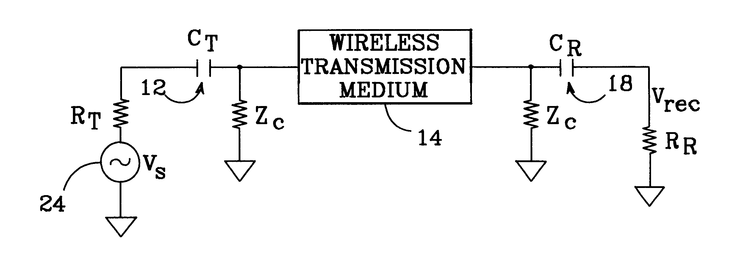
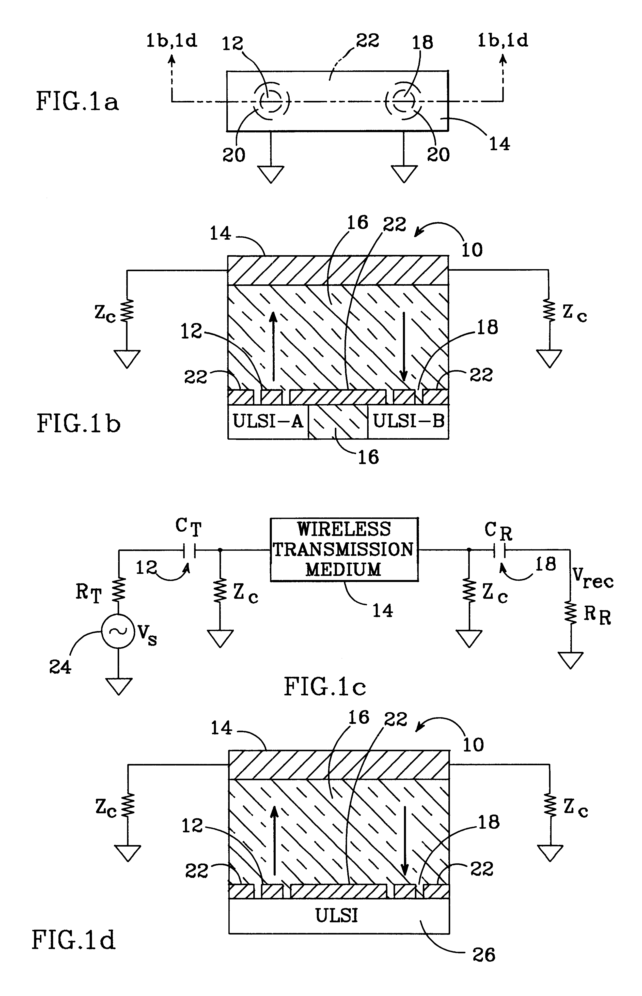
The basic principles of a wireless interconnection system in accordance with the present invention are shown in FIGS. 1a and 1b, which show plan and corresponding cross-sectional views of a package 10 which employs the present invention. The package includes two integrated circuits ULSI-A and ULSI-B which require interconnection. In this example, ULSI-A produces a signal which must be conveyed to ULSI-B. Conventionally, such a signal would be conveyed via a metal interconnect or a wire bond. Here, however, the signal is conveyed wirelessly. The signal from ULSI-A is modulated and routed to a first capacitive coupler 12, which capacitively couples the signal to a wireless transmission medium 14. The wireless transmission medium is physically separated from the ICs, and the ICs separated from each other, with a dielectric filler material 16.

The capacitively coupled signal propagates through wireless transmission medium 14. A second capacitive coupler 18 couples the propagating signal ...


PUM


Abstract

A wireless IC interconnect system and method facilitates interconnections between first and second IC locations via a wireless transmission medium; the IC locations may be on the same chip or on separate chips. A signal to be conveyed is modulated, and the modulated signal is capacitively coupled to the wireless transmission medium—preferably a properly terminated microstrip transmission line (MTL) or a coplanar waveguide (CPW). The modulated signal is capacitively coupled from the wireless medium to a receiver which demodulates the modulated signal and provides the demodulated signal to the second IC location. In a preferred embodiment, the wireless transmission system conveys numerous signals simultaneously, with the signals modulated and demodulated with multiple access algorithms such as code-division (CDMA) and/or frequency-division (FDMA) multiple access algorithms. The interconnection system can be made reconfigurable, with the destinations of the modulated signals changed by reprogramming associated address codes.

Description

BACKGROUND OF THE INVENTION1. Field of the InventionThis invention relates to the field of integrated circuit (IC) interconnections, and particularly to wireless systems and methods of effecting inter- and intra-chip interconnections.2. Description of the Related ArtFor the past three decades, the performance of ICs has depended primarily on device properties. To enhance circuit and system performance, considerable effort has been expended on improving device speed by reducing the device dimensions. This decrease in minimum feature size has led to a proportional decrease in the cross-sectional area and pitch of metal interconnects (“wires”). As a result, the parasitic resistance, capacitance and inductance associated with an IC's wires are beginning to adversely affect circuit performance, and have increasingly become a primary stumbling block in the evolution of deep sub-micron ultra-LSI (ULSI) technology. Recent studies have indicated that when feature sizes fall below 1 μm, the i...

Claims


Application Information

Patent Timeline
IPC IPC(8): H04B5/02
CPCH04B5/02H04B5/0012
Inventor CHANG, MAU-CHUNG F.ITOH, TATSUOQIAN, YONGXIWANG, KANG L.
Owner SILICON STORAGE TECHNOLOGY
Why Eureka
Try Eureka