Thermoelectric material and method of manufacturing the same

a technology of thermoelectric materials and manufacturing methods, applied in the field of thermoelectric materials, can solve problems such as difficulty in attaining

Inactive Publication Date: 2005-02-22
JAPAN AVIATION ELECTRONICS IND LTD
View PDF17 Cites 46 Cited by
  • Summary
  • Abstract
  • Description
  • Claims
  • Application Information

AI Technical Summary

Benefits of technology

It is an object of the present invention to provide a thermoelectric material having a new and novel substance structure in which Seebeck coefficient S and the electrical resistivity ρ thereof can be controlled to get the maximum thermoelectric figure of merit Z as well as the thermal conductivity κlattice thereof can be reduced down to the same level as that of a glass material.
It is a further object of the present invention to provide a method of manufacturing a thermoelectric material having a new and novel substance structure in which Seebeck coefficient S and the electrical resistivity ρ thereof can be controlled to get the maximum thermoelectric figure of merit Z as well as the thermal conductivity κlattice thereof can be reduced down to the same level as that of a glass material.

Problems solved by technology

Incidentally, almost all of thermoelectric materials that have been practically used until now have been semiconductors, and yet have been limited to degenerate semiconductors having high mobility as cited above.
Accordingly, it is difficult to attain a design for substance in which S, ρ and κlattice can be individually controlled to greatly improve the efficiency of thermoelectric conversion, and it has not been materialized to put a thermoelectric material having large ZT, such as beyond 1.5, to practical use.

Method used


Image

  • Thermoelectric material and method of manufacturing the same
  • Thermoelectric material and method of manufacturing the same
  • Thermoelectric material and method of manufacturing the same

Examples


Embodiment Construction

Now, preferred embodiments of the present invention will be described in detail with reference to FIGS. 1 to 3. This invention may, however, be embodied in many different forms and should not be construed as limited to the embodiments set forth hereinafter; rather, these embodiments are provided so that this disclosure will be thorough and complete, and will fully convey the scope of the invention to those skilled in the art.

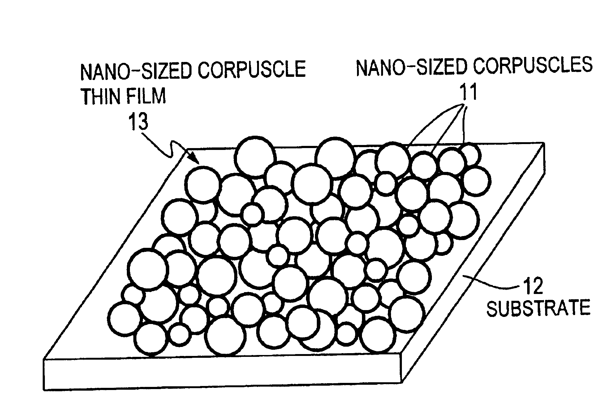
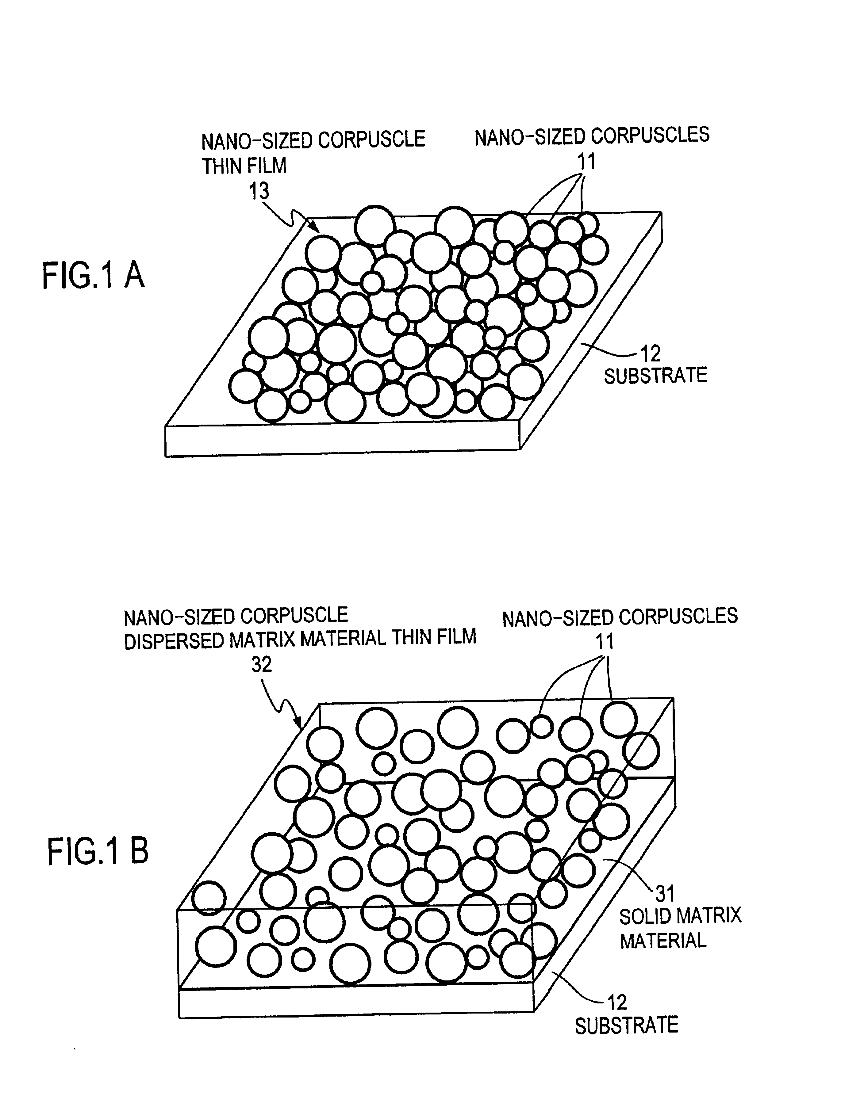
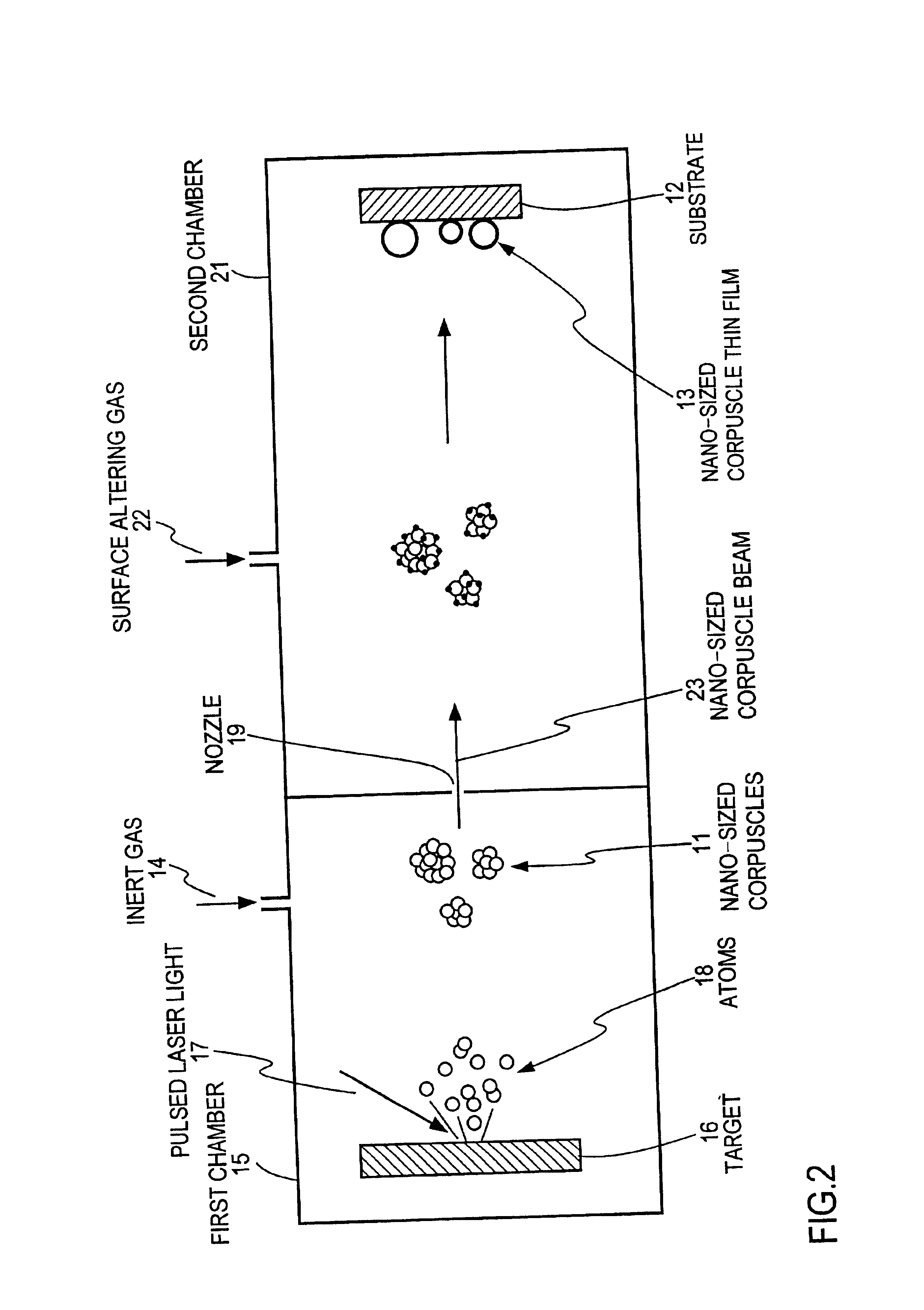
FIG. 1A is an illustrational perspective view showing the constitution of a first embodiment of the thermoelectric material according to the present invention, and FIG. 2 is an illustrational perspective view for explaining a process of manufacturing the thermoelectric material of the first embodiment. As shown in FIG. 1A, the thermoelectric material of this embodiment consists of a thin film of nanometer-sized fine particles 13 formed by depositing on a substrate 12 only nanometer-sized fine particles 11 having their sizes (particle diameters) distributed withi...


PUM

PropertyMeasurementUnit
diametersaaaaaaaaaa
diametersaaaaaaaaaa
pressureaaaaaaaaaa

Abstract

A thermoelectric material having large thermoelectric figure of merit is provided. A thin film comprising nanometer-sized particles having their diameters distributing within the range of 0.5 nm though 100 nm both inclusive is formed by depositing the nanometer-sized particles on a substrate, or dispersing the particles in a solid matrix material or solution thereby to form a thin film. In the thin film, a band gap due to quantum confinement effect is generated in each of the particles and electrical conduction occurs by that at least a part of the particles supply carriers. Accordingly, thermal conductivity κ as well as electrical resistivity ρ and Seebeck coefficient S all of which are factors of thermoelectric figure of merit can be independently controlled, and it is possible to get a thermoelectric material having large dimensionless thermoelectric figure of merit ZT such as beyond 1.5.

Description

BACKGROUND OF THE INVENTION1. Field of the InventionThe present invention relates to a thermoelectric material consisting of a substance having a new and novel structure and / or configuration and a method of manufacturing the thermoelectric material.2. Description of the Related ArtHeretofore, chalcogenide system materials such as Bi2Te3, PbTe and the like, Si—Ge system mixed crystal materials, or the like have been taken up as thermoelectric materials. Thermoelectric figure of merit Z that determines the efficiency of thermoelectric conversion in a thermoelectric material is expressed by the following equation using thermal conductivity κ, electrical resistivity ρ and Seebeck coefficient (thermally generated electromotive force per unit temperature difference) S.Z=S2 / κρThe figure of merit Z has a dimension that is the reciprocal of temperature T, and there are many cases that the product ZT of the figure of merit Z and the temperature T is used as the dimensionless or zero-dimension...

Claims


Application Information

Patent Timeline
Patent Type & Authority Patents(United States)
IPC IPC(8): C23C14/28H01L35/00H01L35/34H01L21/203H01L35/14H01L35/16H01L35/18
CPCC23C14/228C23C14/28H01L35/34Y10T428/29Y10S257/93H10N10/01
Inventor SUZUKI, AKIKOKATAOKA, IZUMI
Owner JAPAN AVIATION ELECTRONICS IND LTD
Why Eureka
Try Eureka