Methods of producing a heterogeneous semiconductor structure

a semiconductor structure and heterogeneous technology, applied in the field of heterogeneous structures, can solve the problems of plastic deformation, delamination or detachment of the substrate, least one of the two substrates breaking, etc., and achieve the effect of improving the quality of the bond and reducing the curvature or deformation

Active Publication Date: 2005-02-22
S O I TEC SILICON ON INSULATOR THECHNOLOGIES
View PDF17 Cites 39 Cited by
  • Summary
  • Abstract
  • Description
  • Claims
  • Application Information

AI Technical Summary

Benefits of technology

The method is advantageously applicable to process substrates at least one of the substrates is formed from a semiconductor material. The use of a stiffening substrate on the first or second substrate substantially reduces the curvature or deformations caused by differences in the coefficients of thermal expansion between the first and the second substrates. In particular, a curvature may occur due to a rise in temperature that is used to de

Problems solved by technology

When the thickness of the substrates is comparable, substantially identical or close to each other and when they behave as thin layers, variations in the behavior of one of the two surfaces with respect to the other can then result in at least one of the two substrates breaking due to a stress release phenomenon.
These temperature variations can also cause delamination or detachment of

Method used


Image

  • Methods of producing a heterogeneous semiconductor structure
  • Methods of producing a heterogeneous semiconductor structure
  • Methods of producing a heterogeneous semiconductor structure

Examples


Embodiment Construction

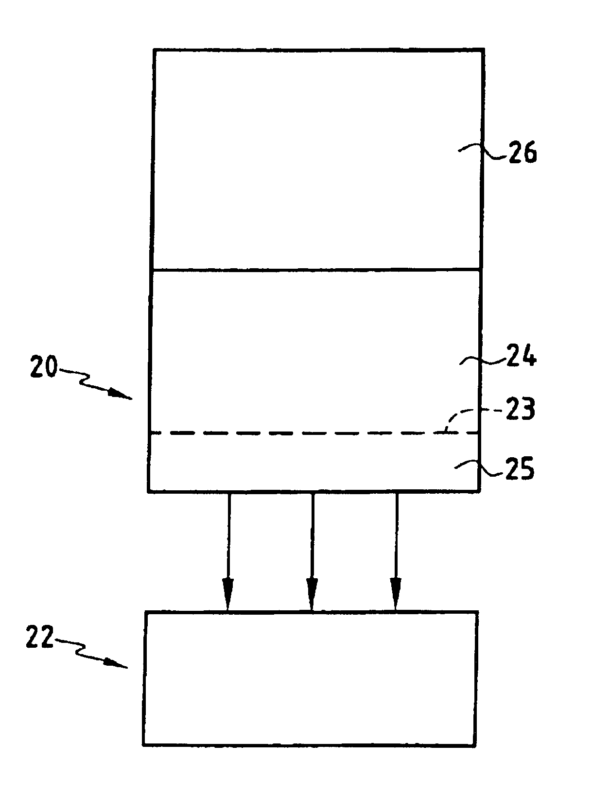
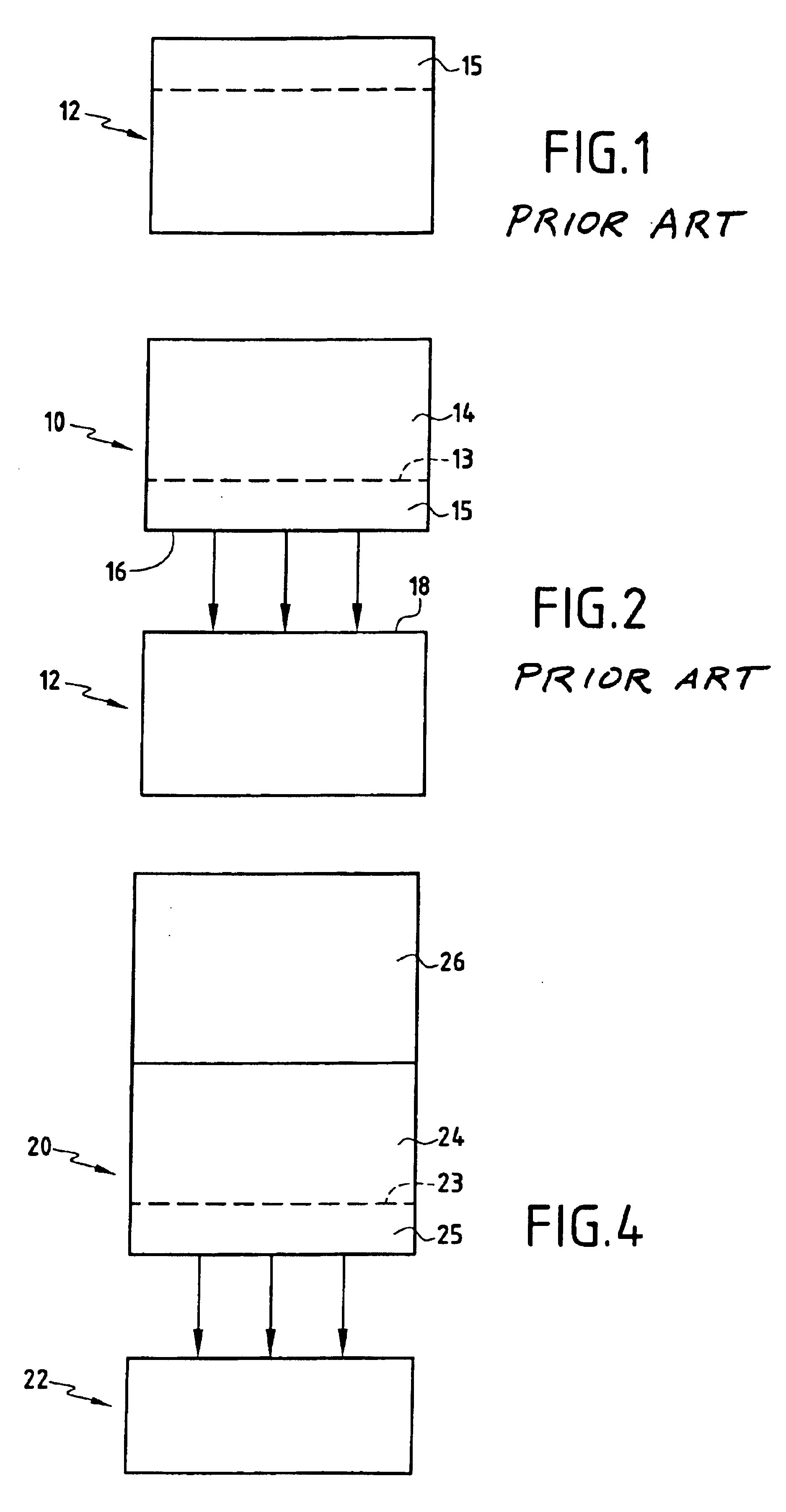
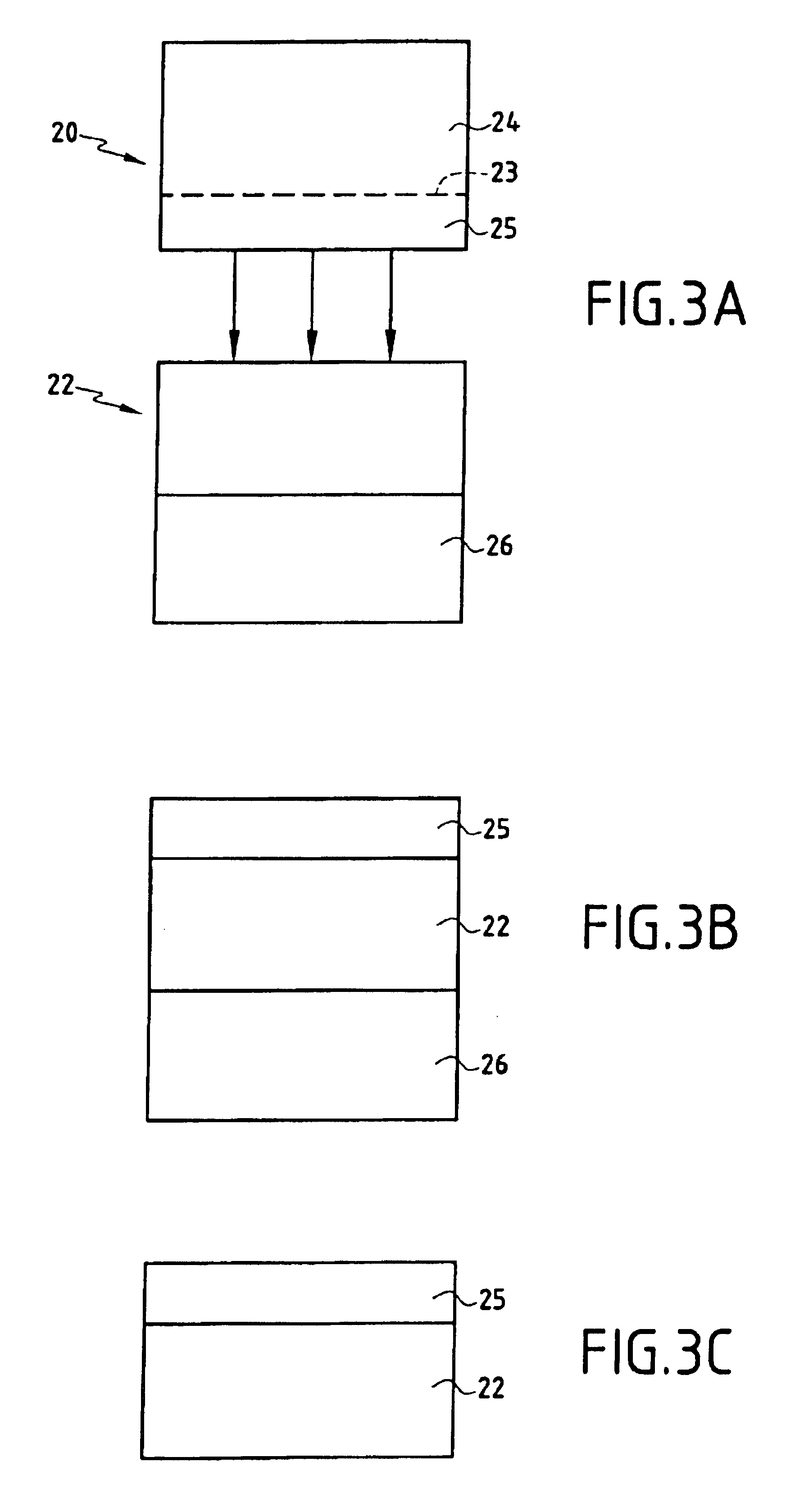
A first example of an implementation of the present method is illustrated by FIGS. 3A to 3C. In FIG. 3A, a first substrate 20 is formed from a first material, and a second substrate 22 having a thickness in the range from about 500 μm to about 1200 μm is formed from a second material. The second substrate has a coefficient of thermal expansion that is different that that of the first substrate. For example, at ambient temperature the relative difference between the two coefficients of thermal expansion is at least about 10% but can be about 20% or even more.

In one example, the first substrate is formed from silicon and the second substrate is formed from quartz. It is also possible to have a silicon-sapphire or silicon-glass type assembly.

In a first step (FIG. 3A), atomic or ionic implantation is carried out on the substrate 20 to form a zone of weakness 23 or fracture zone. The volume of the substrate 20 is thus separated into a lower region 25 (with a thickness in the range of abo...


PUM


Abstract

The present invention relates to a method for forming a heterogeneous assembly of first and second materials having different coefficients of thermal expansion. The method includes bonding a surface of a first substrate of a first material to a surface of a second substrate of a second material wherein the first substrate includes a zone of weakness therein to define a transfer layer adjacent the first surface, providing a stiffening substrate of a third material to maintain sufficient flatness and prevent breakage of the transfer layer during detachment from the first substrate, and detaching the transfer layer from the first substrate along the zone of weakness to form a heterogeneous assembly of the transfer layer and second substrate. The stiffening substrate is bonded to one of the first or second substrates and the third material has a coefficient of thermal expansion that is the same as or close to that of the material of the substrate to which the stiffening substrate is bonded to facilitate a successful detachment of the transfer layer from the first substrate.

Description

BACKGROUND ARTThe invention generally relates to the field of heterogeneous structures. In particular, the invention pertains to methods of forming an assembly that includes a layer of a first material having a first coefficient of thermal expansion on a second substrate of a second material having a different second coefficient of thermal expansion. These methods are useful in forming semiconductor assemblies.A known structure having two substrates with different coefficients of thermal expansion is shown in FIG. 1. The structure includes a substrate 12 with a first coefficient of thermal expansion and a film or layer 15 having a second coefficient of thermal expansion. A quartz-on-silicon system, which can be used in optical applications such as in the production of displays, is one example of such a structure. Silicon has a coefficient of thermal expansion of 3.59×10⁻⁶ / C., and that of quartz is 6×10⁻⁷ / C. Other examples are silicon-on-sapphire, silicon-on-glass, silicon carbide-on...

Claims


Application Information

Patent Timeline
IPC IPC(8): H01L21/70H01L21/762H01L21/02H01L21/265H01L27/12
CPCH01L21/76259H01L21/76254H01L21/76251
Inventor MARTINEZ, MURIELBOUSSAGOL, ALICE
Owner S O I TEC SILICON ON INSULATOR THECHNOLOGIES
Why Eureka
Try Eureka